

PCB Manufacturing & Assembly Capabilities
Know Lianyuhong's Capabilities & Get your PCBs Built Fast. From quick-turn prototypes to high-volume production across all PCB technologies.
Our Services
Comprehensive PCB manufacturing and assembly solutions under one roof.
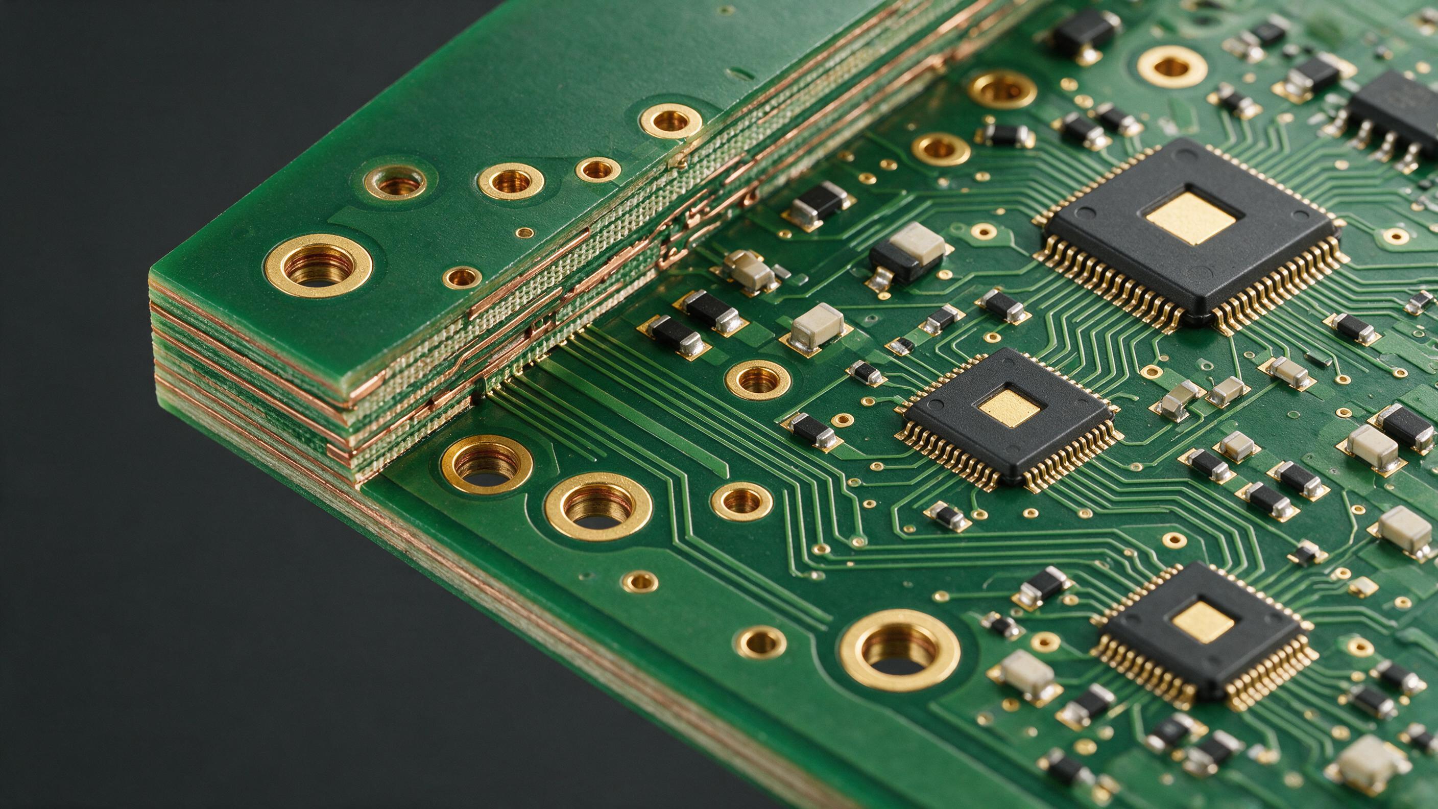
FR-4, High-Tg, Halogen Free, 1-24 layers
High Density Interconnect, Anylayer, 4-24 layers
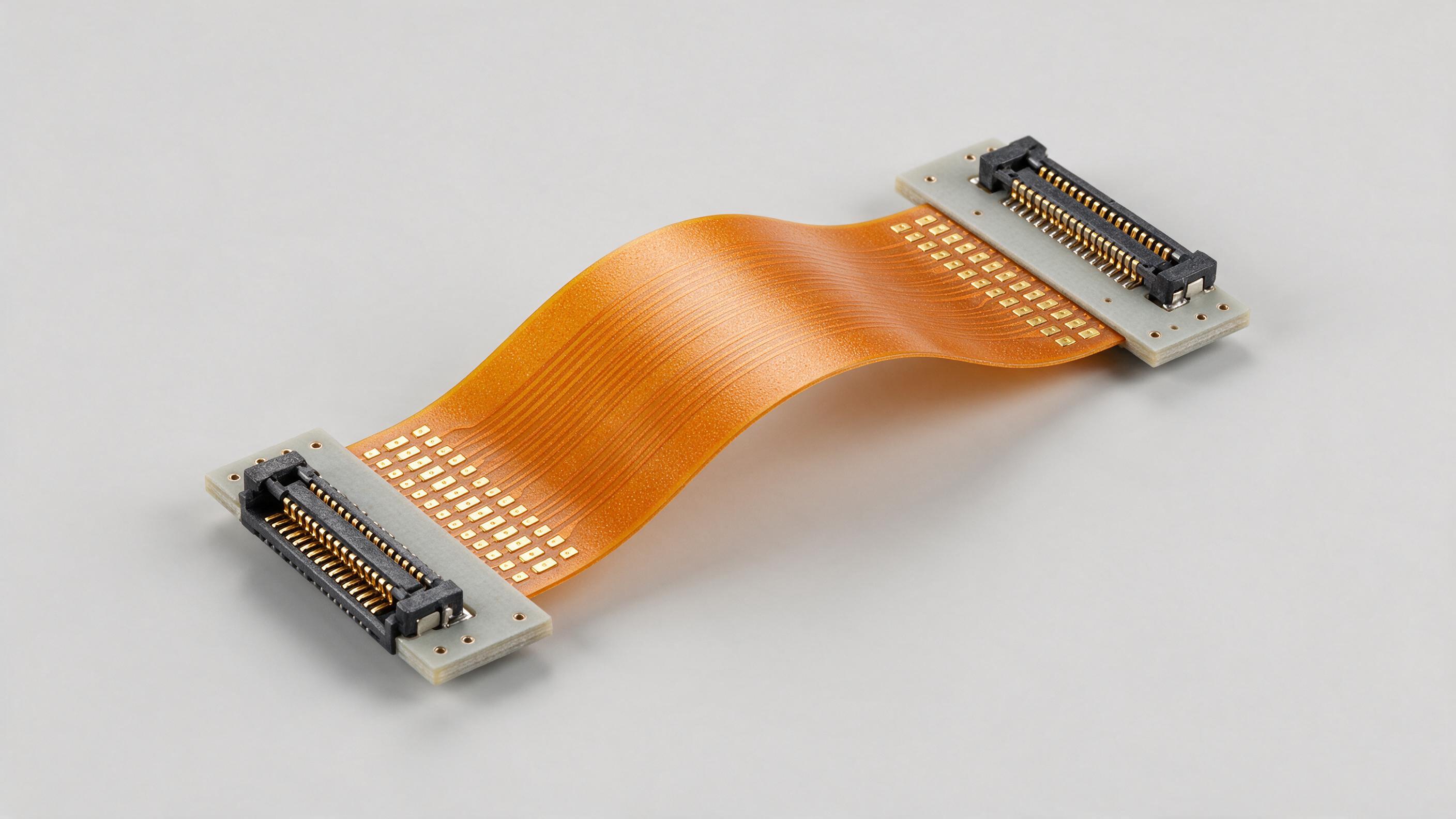
FPC 1-8 layers, Rigid-Flex 2-14 layers
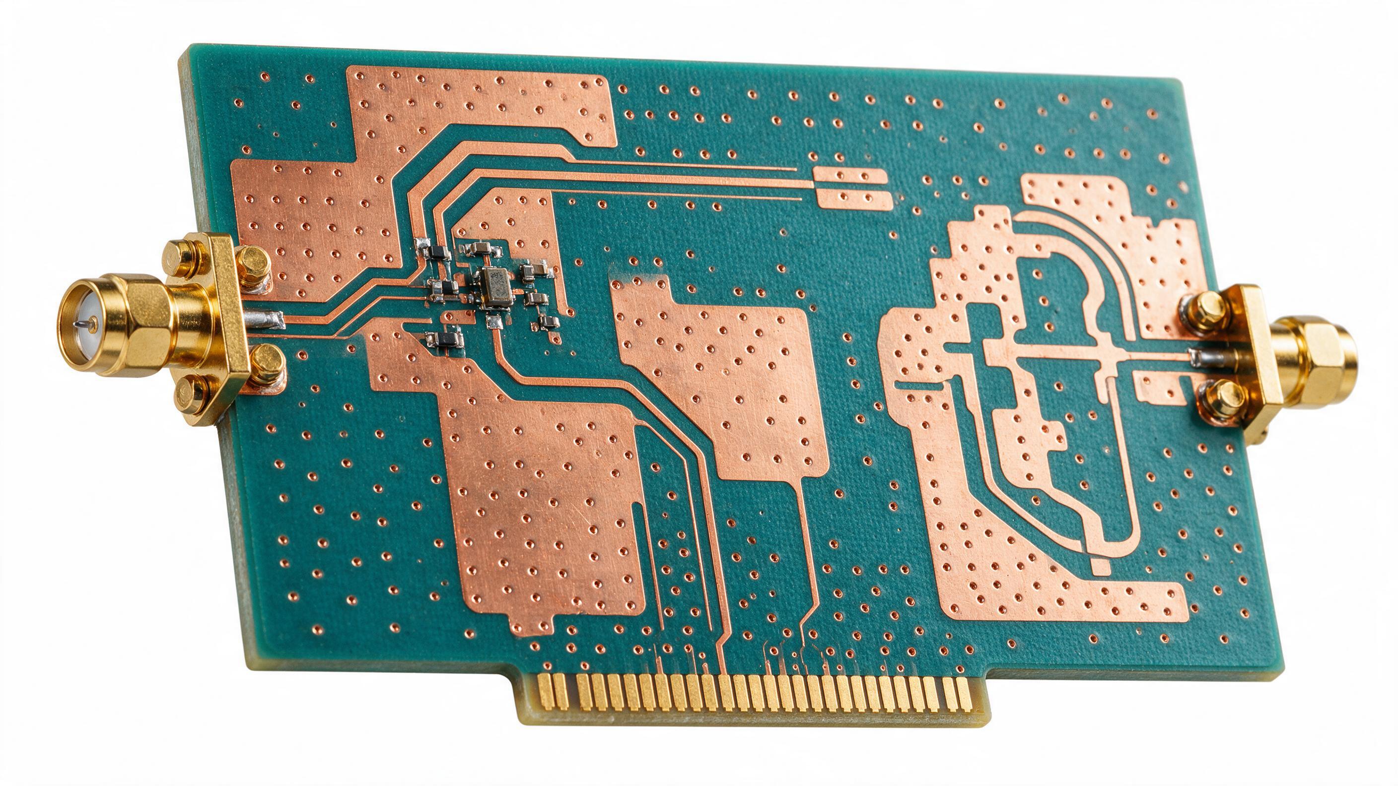
Rogers, PTFE, High-Speed materials
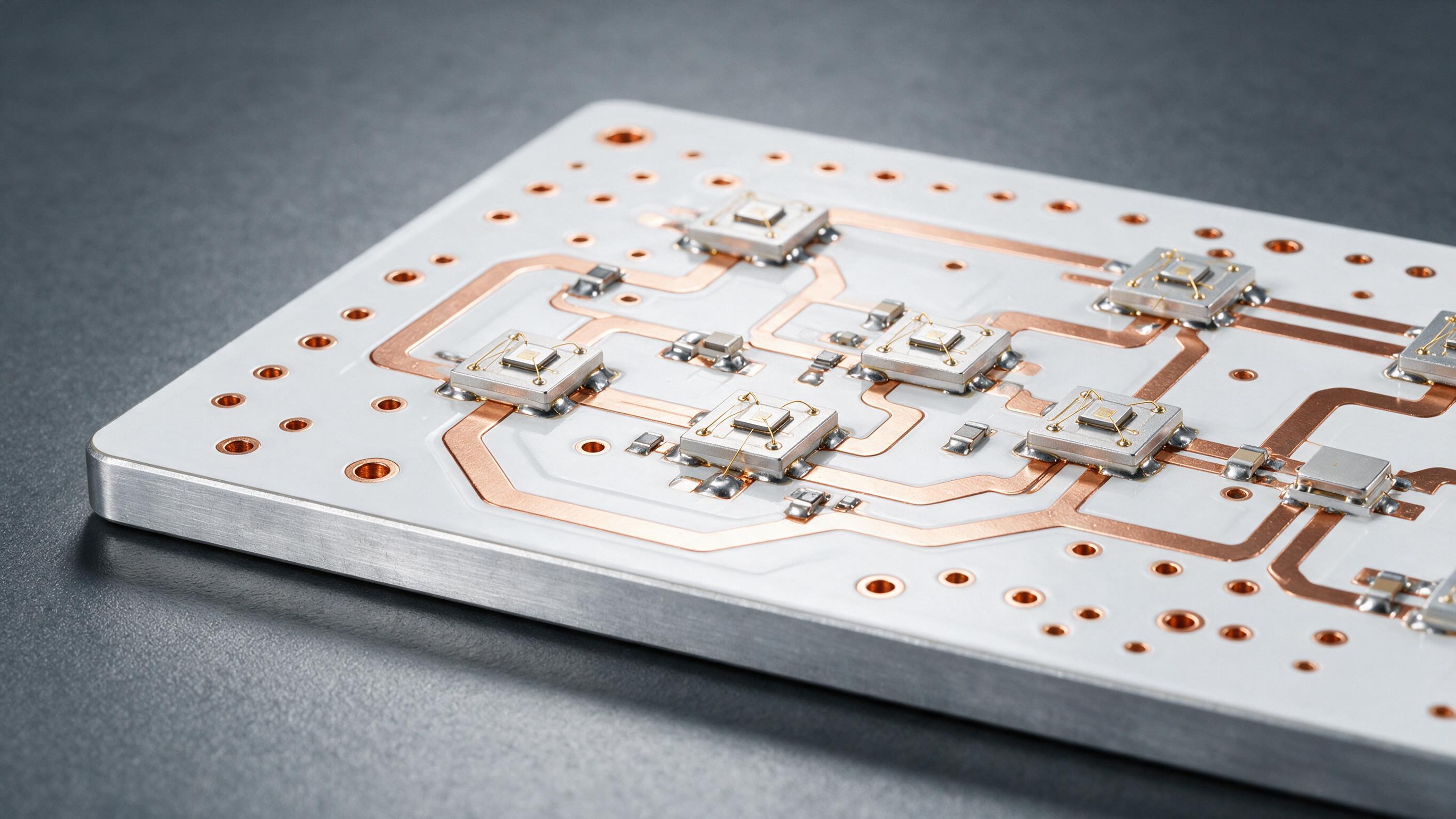
Aluminum & Copper base, 1-2 layers
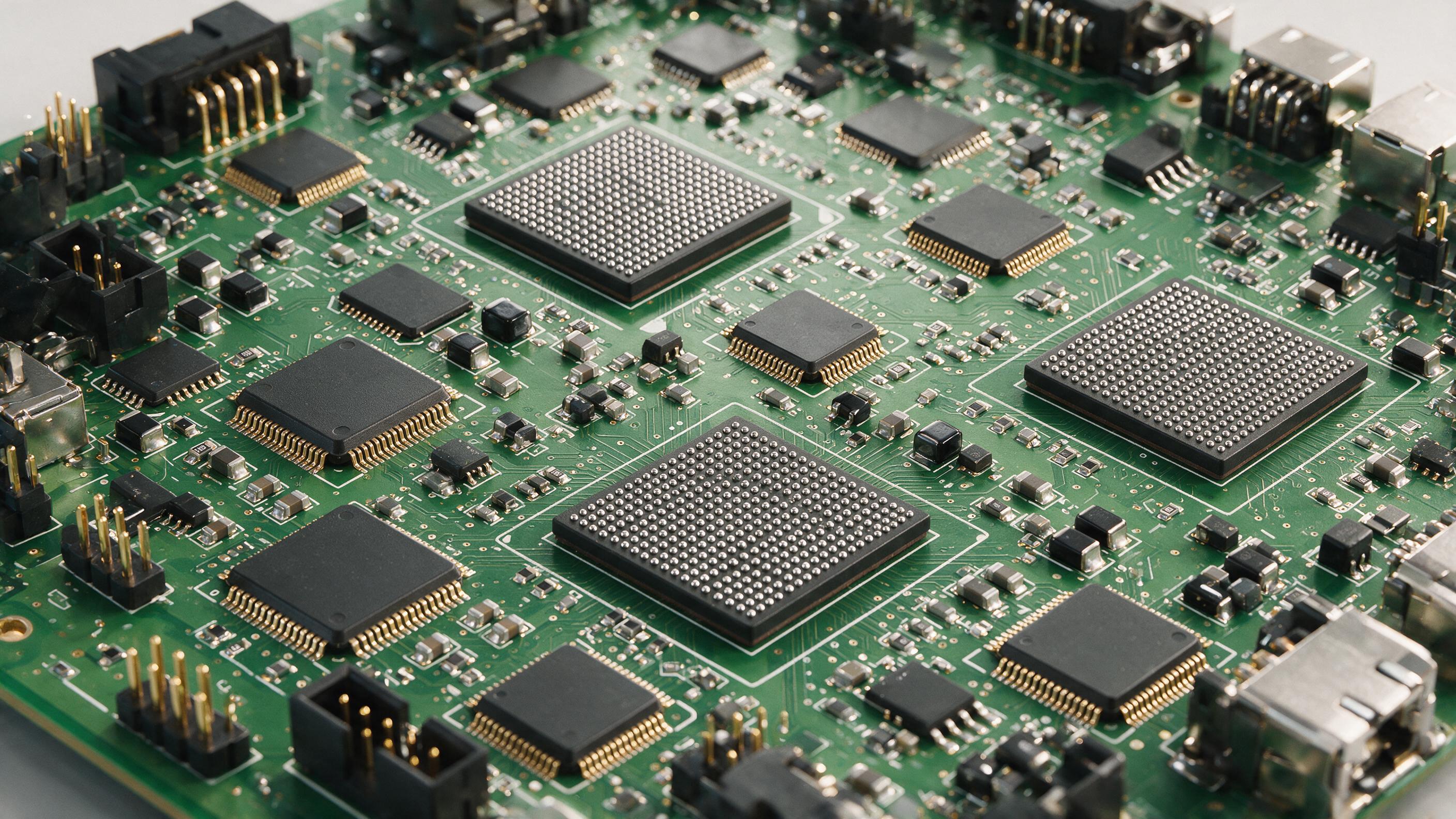
SMT, THT, BGA, Full Turnkey
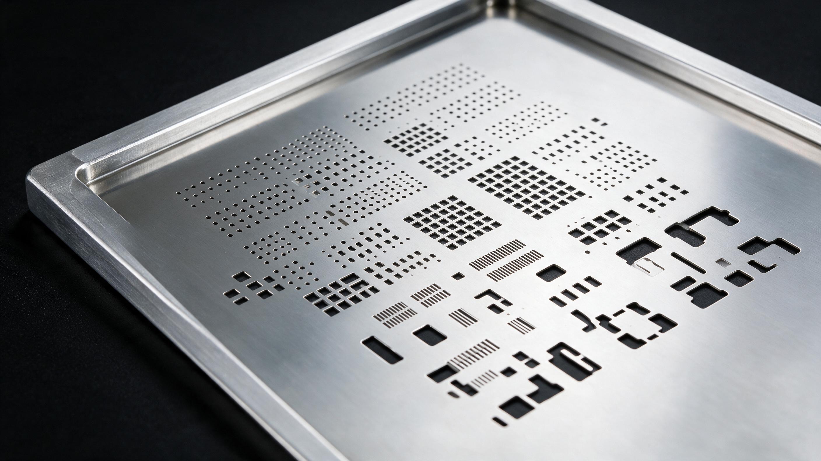
Laser-Cut Stainless Steel Stencils
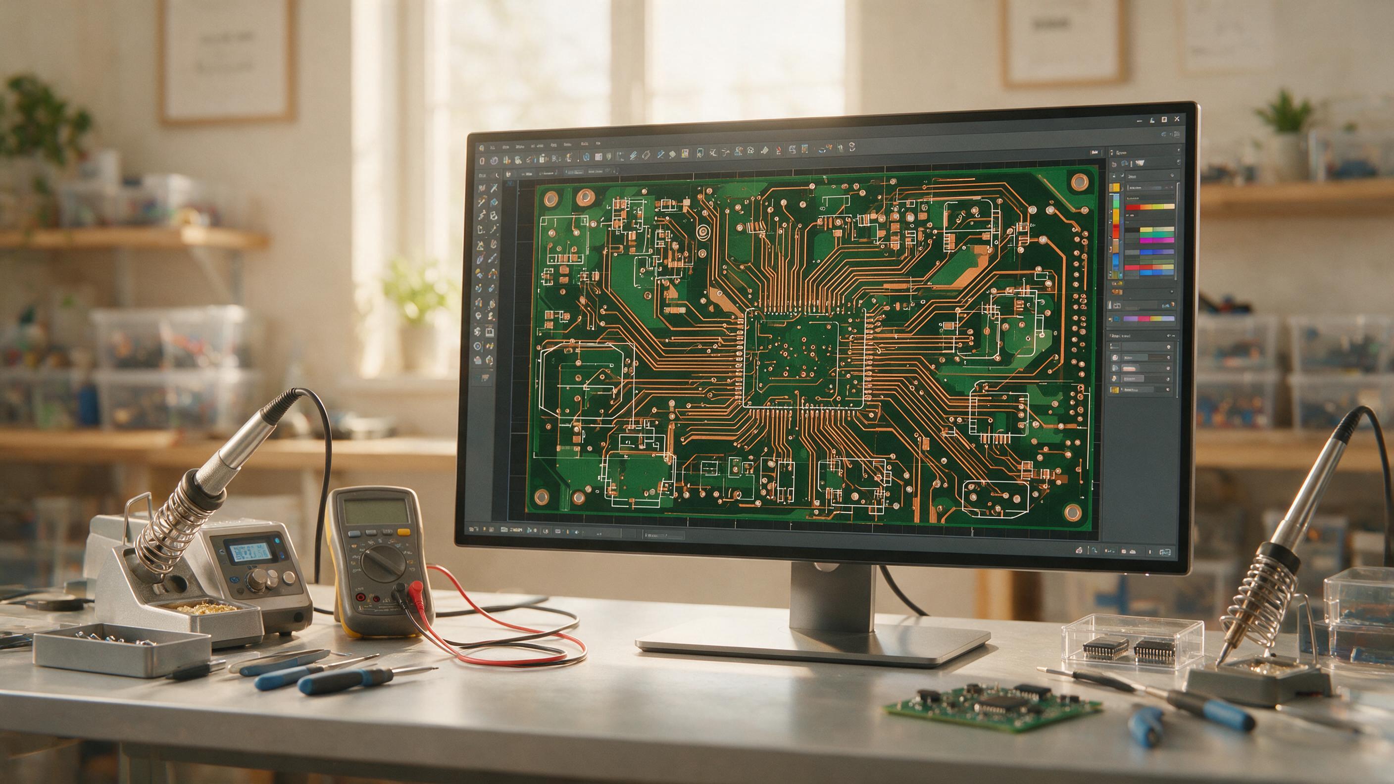
Schematic, Layout, SI/PI, DFM Review
PCB Manufacturing Capabilities
Technical specifications across our four main PCB manufacturing platforms: HLC (High Layer Count), HDI (High Density Interconnect), FPC & Rigid-Flex, and IMS (Insulated Metal Substrate).
| Feature | HLC (1-24L) | HDI (4-24L) | FPC & Rigid-Flex | IMS (1-2L) |
|---|---|---|---|---|
| Layer Count | 1 – 24 | 4 – 24 | FPC: 1 – 8 Rigid-Flex: 2 – 14 | 1 – 2 |
| Board Thickness (mm) | 0.3 – 3.4 | 0.27 – 3.4 | FPC: 0.05 – 1.0 Rigid-Flex: 0.27 – 3.2 | Typical: 1.6 Max: 3.2 Min: 0.8 |
| Min Dielectric Thickness (mm) | 0.05 | 0.05 | 0.05 | 0.05 |
| Max Panel Size (mm) | 724 × 622 (28.5" × 24.5") | 610 × 475 (24" × 18.7") | FPC: 250 × 550 Rigid: 500 × 600 | 520 × 610 (20.5" × 24.0") |
| Base Copper (oz) | 0.5 / 1 / 3 / 6 | 0.5 / 1 / 3 / 4 | FPC: 1/3 – 2 Rigid-Flex: 1/3 – 4 | / |
| Finished Copper Outer (oz) | 1 – 5 | 1 – 2 | 1 – 2 | 1 – 2 |
| Hole-wall Copper (μm) | 20 – 70 | 20/18, 25/20 | 20 / 25 | 20 / 25 |
| Min Line/Space Inner (mm) | 0.05 / 0.05 | 0.05 / 0.05 | FPC: 0.04 / 0.04 | / |
| Min Line/Space Outer (mm) | 0.05 / 0.05 | 0.05 / 0.05 | FPC: 0.045 / 0.045 Rigid-Flex: 0.05 / 0.05 | 0.10 / 0.10 |
| Line Width Tolerance | ±20% (Typical) ±10% (Advanced) | ±20% (Typical) ±10% (Advanced) | ±20% (Typical) ±10% (Advanced) | ±20% (Typical) ±10% (Advanced) |
| Layer Registration (mil) | 5 | 5 | 5 | 5 |
| Impedance Tolerance | ±8% | ±8% | ±8% | / |
| Min Mechanical Drill (mm) | ≥0.15 | ≥0.15 | ≥0.15 | 1 – 6 |
| Min Laser Drill (mm) | ≥0.075 | ≥0.075 | ≥0.075 | / |
| Max Aspect Ratio (PTH) | 12:1 | 12:1 | 12:1 | 4:1 |
| Max Aspect Ratio (Microvia) | / | 1:1 | 1:1 | / |
| Backdrill Tolerance (mil) | ±3 | ±3 | ±3 | ±4 |
Laminate Materials
Standard Suppliers
Rogers, Panasonic, Nelco, TUC, Isola, ITEQ, SYTECH, Nanya, Taconic, EMC, DOOSAN, Wazam, CCTC, NOUYA, KB
Flex Suppliers
SYTECH, TAIFLEX, ThinFlex
IMS Suppliers
Wazam, Ventec, ITEQ, SYTECH, RISHO
Material Types
Surface Finish
Standard Options
HASL-LF, HASL, ENIG (Electroless Nickel/Immersion Gold), Immersion Tin, OSP, Immersion Silver, Gold Finger, Selective OSP
IMS Options
HASL-LF, ENIG, OSP
Signal Integrity
SET2DIL, Delta-L, and VNA (Vector Network Analyzer) based verification for high-speed and high-frequency designs.
Drilling & Vias
| Feature | Capability | Description |
|---|---|---|
| Min. Mechanical Drill Diameter | ≥0.15 mm (HLC/HDI/FPC) 1 – 6 mm (IMS) | Minimum mechanical drill size for standard boards. IMS PCBs require 1-6mm drills. |
| Min. Laser Drill Diameter | ≥0.075 mm | Laser microvia drilling for HDI and high-density designs. |
| Max. Aspect Ratio (PTH) | 12:1 (HLC/HDI/FPC) 4:1 (IMS) | Plated through-hole aspect ratio. Higher ratios available on advanced HDI builds. |
| Max. Aspect Ratio (Microvia) | 1:1 | Laser microvia aspect ratio for HDI builds. |
| Hole-wall Copper Thickness | 20 – 70 μm (HLC) 20/25 μm (FPC/IMS) | Copper plating thickness in plated through holes. |
| Backdrill Depth Tolerance | ±3 mil (HLC/HDI/FPC) ±4 mil (IMS) | Controlled depth backdrilling for high-speed signal integrity. |
| Blind / Buried Vias | Supported | HDI builds support blind, buried, stacked, and staggered vias. Anylayer HDI available. |
| Layer to Layer Registration | 5 mil | Registration accuracy between layers. |
Traces & Impedance
| Feature | Capability | Description |
|---|---|---|
| Min. Track / Space (Inner) | 0.05 / 0.05 mm (HLC/HDI) 0.04 / 0.04 mm (FPC) | Minimum trace width and spacing for inner layers. |
| Min. Track / Space (Outer) | 0.05 / 0.05 mm (HLC/HDI/Rigid-Flex) 0.045 / 0.045 mm (FPC) 0.10 / 0.10 mm (IMS) | Minimum trace width and spacing for outer layers. |
| Track Width Tolerance | ±20% (Typical) ±10% (Advanced) | Standard and advanced tolerance for trace width control. |
| Controlled Impedance | ±8% | Impedance control with SET2DIL / Delta-L / VNA verification. |
| Min. BGA Pitch | 0.35 mm (HDI) 1.0 mm with backdrill | 0.35mm pitch BGA requires HDI technology and ENIG surface finish. |
Special Processes
Embedded PCB
Embedded parallel capacitor, Embedded daughter board
Stepped PCB
PTH slot, NPTH slot, Stepped Gold Finger
Heat Dissipation PCB
IMS, Embedded Cu/Coin/Ceramic, Conductive Adhesive, High Thermal Dissipation Material, Heat Sink Paste
High Density PCB
1mm pitch BGA with backdrill (2 tracks), 8mil PTH with backdrill (D+6mil), 0.35mm pitch BGA HDI
Other Special Processes
POFV (VIPPO), Hybrid, Partial Hybrid, Variable Length G/F, Stepped G/F, Segmented G/F, Edge Plating, N+N, Partial Plating, Semi-flex
HDI Structures
Through hole, 5+N+5 Common Symmetrical, Symmetrical HDI, Air-gap Structure, Anylayer, Asymmetric HDI
PCB Assembly
| Feature | Capability | Description |
|---|---|---|
| Assembly Type | SMT, THT, Mixed | Single-sided, double-sided, and mixed-technology assembly. |
| Min. SMT Component Size | 01005 (0.4 × 0.2 mm) | Supports 01005, 0201, 0402, 0603, 0805, 1206, and larger. |
| BGA / QFN Support | Yes | BGA, QFN, QFP, LGA, CSP with X-Ray inspection. |
| Min. BGA Pitch | 0.35 mm (HDI) | 0.35mm pitch BGA with ENIG surface finish and X-Ray verification. |
| Supported PCB Types | FR-4, HDI, Flex, Rigid-Flex, IMS, HF, Hybrid | Full turnkey assembly for all PCB technologies we manufacture. |
| Inspection Methods | SPI, AOI, X-Ray, Flying Probe, FCT | Solder paste inspection, automated optical inspection, BGA X-Ray, electrical and functional testing. |
| Lead Time | 24 hours (prototype) | Standard: 2-5 days. Volume production: 7-15 days. |
| Min. Order Quantity | 1 pc | No MOQ for prototype assembly. |
SMT Stencil
| Feature | Capability | Description |
|---|---|---|
| Material | 304 HTA Stainless Steel | High-tensile annealed stainless steel for precise aperture cutting. |
| Min. Aperture | 0.08 mm | Supports 01005 components and 0.35mm BGA. |
| Cutting Tolerance | ±0.003 mm | Laser-cut precision with smooth aperture walls. |
| Build Time | 12 hours | Standard stencil build time. Express options available. |
| Finish Options | Nano Coating / Electropolish | Nano coating for faster paste release. Electropolish for smooth walls. |
| Thickness Range | 0.08 – 0.3 mm | Standard 0.1mm, 0.12mm, 0.15mm, 0.18mm, 0.2mm, 0.25mm, 0.3mm available. |
| Max. Stencil Size | 736 × 736 mm (29" × 29") | Supports large panel printing. |
PCB Layout & Design
| Feature | Capability | Description |
|---|---|---|
| Design Software | Altium, Cadence, Mentor, KiCad, Eagle | Industry-standard EDA tools for all design complexity levels. |
| Max Layers | 24 layers | Aligned with our manufacturing capabilities. |
| Min. Track/Space | 0.04 mm (Flex) / 0.05 mm (Rigid) | Precision routing for HDI and high-density designs. |
| Impedance Control | ±8% with SI verification | Controlled impedance design with SET2DIL/Delta-L/VNA verification. |
| HDI Design | Anylayer, 5+N+5, Blind/Buried Vias, Backdrill | Full HDI design capability including advanced structures. |
| Technologies | Rigid, Flex, Rigid-Flex, HDI, IMS, High-Frequency | Design for all PCB technologies including Rogers/PTFE materials. |
| Output Formats | Gerber RS-274X, ODB++, IPC-2581, DXF | All standard manufacturing output formats supported. |
Ready to Start Your PCB Project?
Upload your design files and let our team provide a competitive quote within 24 hours.