
A real HDI PCB manufacturer is worth choosing only when they can show documented microvia construction, controlled-impedance evidence, and process controls that survive lead-free reflow. China generated approximately US$22.98 billion of PCB output in 2023, with HDI boards at 27.8% of mainland China's PCB output, so you're not shopping for a niche process, you're choosing a supplier that has to prove it can hold up under real volume pressure.
You're probably at the point where the schematic is frozen, the BGA pitch is tight, and the easy board houses have already told you no. The right move now is to stop asking who can “do HDI” and start asking who can document it.
Table of Contents
- What an HDI PCB Manufacturer Really Builds
- Core Capabilities That Define a Real HDI Shop
- Microvia Reliability and What It Means for Your Design
- From Fabrication to Assembly Under One Roof
- Certifications and Process Controls Worth Reading
- Lead Time, Cost Drivers, and How Quotes Move
- Buyer Checklist, DFM Tips, and Qualifying Questions
<a id="what-an-hdi-pcb-manufacturer-really-builds"></a>
What an HDI PCB Manufacturer Really Builds
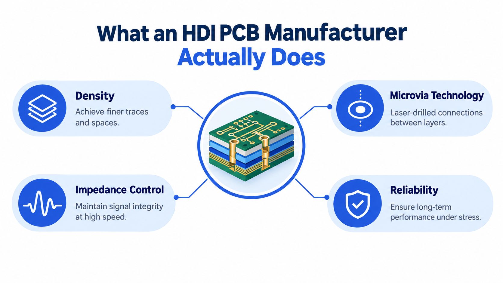
An HDI PCB manufacturer does more than drill smaller holes. The shop has to control microvias, sequential build-up, tight registration, and fine-pitch interconnect density so a board can carry more routing in less space without becoming a reliability problem. That is the practical meaning of HDI, and the process grew because board density kept rising while board size and via dimensions kept shrinking, with early production milestones including laser-drilled FINSTRATE boards in 1984 and Surface Laminar Circuit in Japan in 1991 HDI technology background.
<a id="what-hdi-looks-like-in-a-real-board"></a>
What HDI looks like in a real board
A 10-layer smartphone mainboard with laser-drilled microvias, AnyLayer construction, and 0.35 mm BGA fan-out does not work because a sales sheet says “HDI capable.” It works because the fabricator can hold layer registration, build the interconnect structure, and route the BGA escape without breaking signal integrity or assembly yield.
Practical rule: If the design needs fine-pitch escape routing, ask the fabricator to describe the via stack and registration method in plain English, not just in marketing terms.
HDI is not limited to one device class. It is used across mobile, consumer, telecommunications, computing, automotive, medical, and aerospace applications HDI technology background. That breadth matters because it shows HDI is a manufacturing discipline, not a product category. A supplier should be able to explain laser microvias, AnyLayer structures, backdrilling, and fine-pitch BGA support as part of one process chain, not as isolated menu items.
If your board depends on high-density routing, think in evidence. The question is not whether the shop says it can build HDI. The question is whether the layout, stack-up, and via architecture are manufacturable at the level your design requires.
<a id="core-capabilities-that-define-a-real-hdi-shop"></a>
Core Capabilities That Define a Real HDI Shop
A real HDI shop proves capability through process artifacts, not adjectives. The first thing to check is whether it can support laser microvias, because those are the backbone of dense routing. The second is whether it can build AnyLayer structures, because that tells you it can place interconnects where the design needs them instead of forcing awkward routing compromises.
<a id="capability-versus-proof"></a>
Capability versus proof
Here's the short version: if a shop lists a feature, ask for the document that proves it.
- Laser microvias: Ask for drill file review, via diameter limits, and representative cross-sections that show the drilled and plated structure.
- AnyLayer structures: Ask for the stack-up drawing and an example of sequential build-up that shows how interconnects move between layers.
- Backdrilling: Ask for the backdrill callout on the drawing and the accepted stub-length target for high-speed nets.
- 0.35 mm BGA support: Ask for the fan-out strategy, routing rules, and a layout sample that shows it's not just a theoretical pitch number.
- Controlled impedance: Ask for the impedance coupon report, measurement method, and the tolerance window tied to the actual stack-up.
That's the difference between a fabricator and a supplier that can release production boards. For a program that needs board assembly too, you should check whether the vendor can keep the same discipline from bare board into SMT. If you want a single vendor path, the internal PCB assembly capability overview is the kind of page you should treat as a services map, not as proof.
<a id="what-to-leave-out-of-the-spec"></a>
What to leave out of the spec
Not every HDI design needs every HDI feature. Don't spec stacked complexity just because it sounds advanced. If the routing works with staggered microvias, use them. If a backdrill isn't doing anything for your high-speed nets, don't pay for it.
A serious supplier should help you simplify the design where possible. That usually means fewer build-up cycles, fewer exotic stack-up choices, and tighter focus on the structures your signal paths need. The buyer's job is to separate necessary density from decorative complexity.
<a id="microvia-reliability-and-what-it-means-for-your-design"></a>
Microvia Reliability and What It Means for Your Design
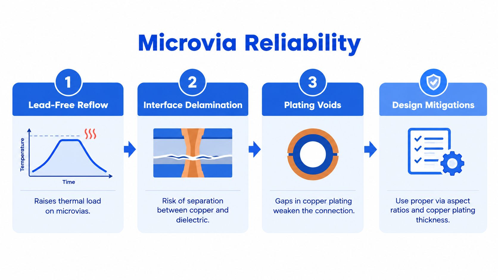
Microvia reliability decides whether an HDI build survives real use or fails after assembly. IPC technical analysis points to two failure drivers, weak metallurgical bonding between electroless copper and the target capture pad, and voids in electrodeposited copper. The same analysis identifies interface delamination as the most common failure mode, and notes that large internal voids can cut microvia fatigue life by more than 90% IPC microvia reliability analysis.
<a id="why-lead-free-assembly-changes-the-risk"></a>
Why lead-free assembly changes the risk
Lead-free assembly raises the thermal load on microvias. IPC reliability work reports failures at the microvia barrel, corners, capture-pad interfaces, and target-pad registration under higher assembly and rework temperatures, using IPC TM-650 2.6.26 interconnect stress methods up to 190°C for FR-4 and 230°C for polyimide test vehicles IPC interconnect stress testing. In the same IPC study, lead-free assembly and rework reduced cycles to failure by 99% in the examined case, and failure analysis tied the result to barrel cracking and contamination or debris at the electroless-copper/capture-pad interface.
A supplier that only shows bare-board images has not demonstrated anything about reflow survival. You need evidence that connects fabrication quality to assembly reality. If the vendor cannot trace the process chain to the failure modes, the “HDI” label is just marketing.
<a id="what-to-demand-before-release"></a>
What to demand before release
The practical design rule is simple. Published technical guidance reports that microvias with an aspect ratio near 0.7:1 survived accelerated testing, while 1:1 structures failed after only a few thermal cycles in the cited study. That does not mean every board should use the same number, but it does mean the smallest possible microvia is not automatically the safest choice.
Request this package: cross-section images, plating thickness, void criteria, thermal-cycle results, and explicit reflow and rework limits.
Stacked microvias need extra scrutiny because they concentrate thermomechanical stress at the buried copper interface. If your board needs them, require documented construction, not a verbal promise. Ask for the representative coupon, the post-test cross-sections, and the failure-analysis record if anything goes wrong.
<a id="from-fabrication-to-assembly-under-one-roof"></a>
From Fabrication to Assembly Under One Roof
HDI stops being a pure fabrication question the moment your board has to be assembled and shipped on schedule. The risk in a split-vendor setup is simple, each handoff creates room for stack-up drift, sourcing mistakes, or test gaps. A turnkey model reduces those handoff losses because one team is managing the design review, the board build, and the assembly release.
<a id="the-chain-you-should-expect"></a>
The chain you should expect
A competent turnkey flow usually runs through DFM review, stack-up sign-off, bare-board fabrication, component sourcing, SMT and THT assembly, inspection, and functional test. Each step can become a schedule gate if the owner changes from one company to another. If the fabricator never sees the assembly constraints, you end up with a board that's technically manufacturable but painful to populate.
| Process Step | What Is Delivered | Common Owner | |---|---|---| | DFM review | Manufacturing feedback on stack-up, vias, and assembly risks | Fabricator or turnkey partner | | Stack-up sign-off | Approved layer and dielectric structure | Engineering and CAM | | Bare-board fabrication | Finished HDI PCB panels | PCB fabricator | | Component sourcing | Traced parts and lot records | Assembly partner or buyer | | SMT and THT assembly | Populated boards with soldered components | EMS or turnkey supplier | | Inspection and test | AOI, X-ray, flying-probe, functional test | Assembly or quality team |
A turnkey partner is the cleaner choice when the program needs compressed scheduling, mixed HDI and assembly risk, or prototype-to-small-batch continuity. A fabricator-only relationship can still make sense if your assembly house already owns the build and you just need the board released on spec.
<a id="where-the-supply-chain-usually-slips"></a>
Where the supply chain usually slips
The weakest point is usually not fabrication itself. It's the gap between the board rules and the assembly rules. A BGA that looks fine on paper can become a sourcing or placement headache if the supplier never aligned the stencil, pad finish, and inspection method with the actual part mix.
Lianyuhong Technology Co.,Ltd offers the kind of combined board and assembly path that fits this model, with rigid, HDI, flexible, high-frequency, and ceramic fabrication alongside turnkey SMT and THT assembly. If you're trying to collapse vendors this quarter, that matters more than a long list of disconnected services.
<a id="certifications-and-process-controls-worth-reading"></a>
Certifications and Process Controls Worth Reading
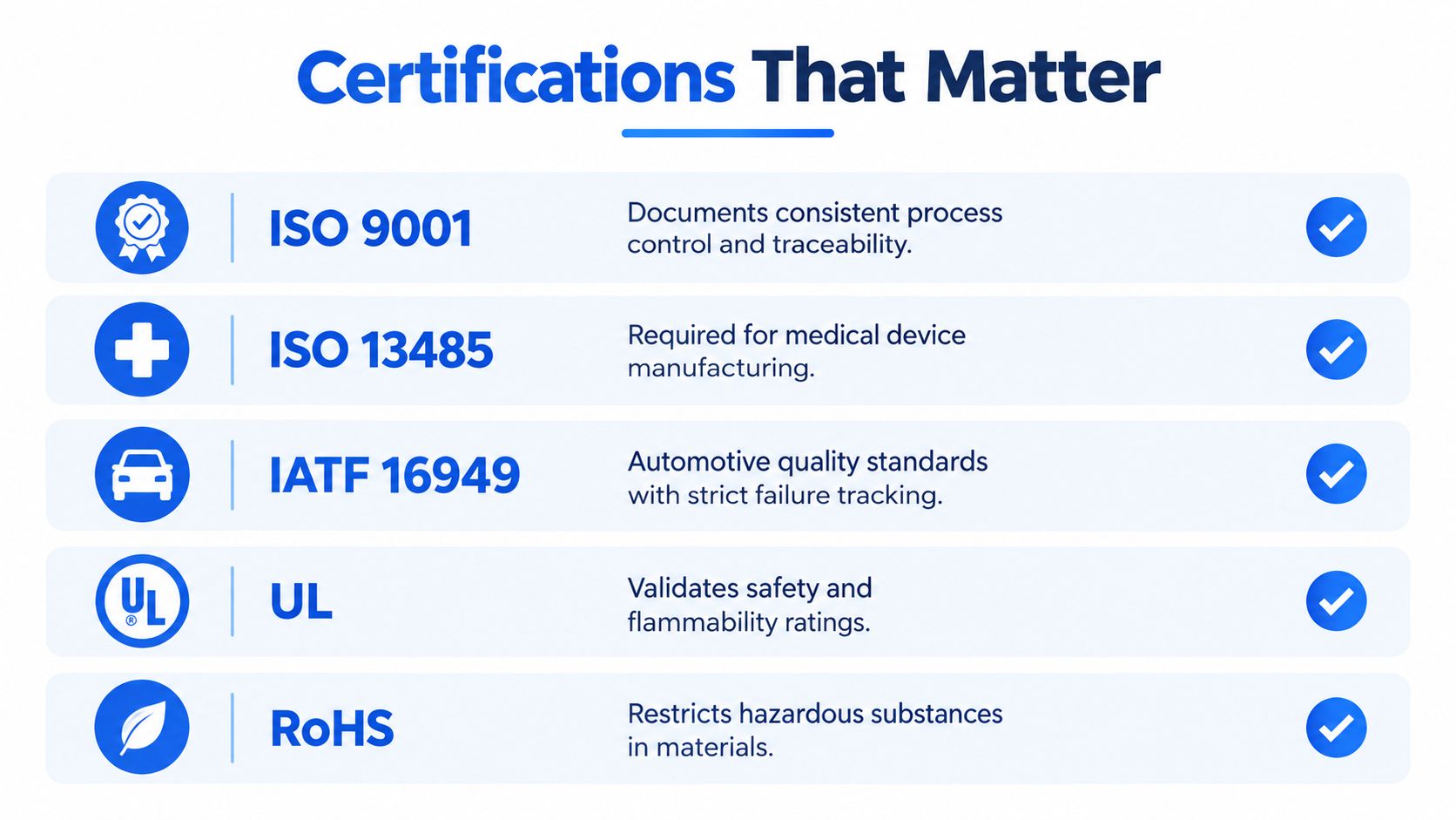
Quality badges matter only when they force the shop to prove control over the board you are buying. ISO 9001 tells you the manufacturer runs a quality management system. ISO 13485 matters for medical device work, IATF 16949 matters for automotive supply, UL affects safety and flammability recognition, and RoHS addresses restricted substances. Read those marks as evidence targets, not decoration.
<a id="read-the-process-controls-not-just-the-logo-strip"></a>
Read the process controls, not just the logo strip
The controls that matter are the ones you can audit. For assembly, ask for SPI data on solder-paste volume, AOI results for visible joints, X-ray coverage for hidden BGA and QFN connections, and flying-probe or functional test records for electrical verification. If the supplier cannot name the method and the output, the certification list is just a wall of logos.
A quality page is useful only when it tells you what gets checked, when it gets checked, and what evidence you can request later.
Controlled impedance deserves the same treatment. If the shop claims ±8 percent tolerance, that claim should sit on a defined stack-up and a stated measurement method. For HDI builds, that is the difference between a controlled release and a board that comes back for re-spin.
<a id="what-good-operational-practice-looks-like"></a>
What good operational practice looks like
Operational detail tells you how the supplier handles pressure. 24-hour prototype assembly when materials are available is worth real money when the schedule is already slipping. No-MOQ small-batch runs help when you need bridge production without overcommitting inventory. Authorized-distributor sourcing with traceable lot records keeps part provenance clean when the build gets audited.
Lianyuhong's documented quality scope is worth reading in that same light, especially through its certification page. If the page shows the right controls, use it to ask for the proof behind them.
<a id="lead-time-cost-drivers-and-how-quotes-move"></a>
Lead Time, Cost Drivers, and How Quotes Move
HDI pricing does not move on layer count alone. Two quotes can look similar on paper and diverge fast once you factor in stack-up complexity, AnyLayer count, via type, aspect ratio, finish, impedance testing, inspection scope, and component sourcing. If you only compare the headline price, you usually pay later in schedule risk or rework.
<a id="the-variables-that-change-the-number"></a>
The variables that change the number
A 10-layer board with AnyLayer routing and 0.35 mm BGA support costs more to build than a simpler multilayer board because the fabricator has to hold tighter registration and add more process steps. Add ENIG and impedance coupon testing, and you are asking for a more controlled build than an OSP board with no impedance verification. That difference is not cosmetic. It changes process time, inspection scope, and the confidence you can put behind release.
| Build choice | What changes | Quote impact | |---|---|---| | ENIG with impedance control | More process control and test documentation | Higher cost, longer lead time | | OSP without impedance control | Simpler finish and less verification | Lower cost, faster quote path | | Complex AnyLayer stack-up | More lamination and registration risk | Higher cost and more schedule sensitivity | | Standard multilayer build | Fewer build-up steps | Lower cost and fewer handoffs |
<a id="why-logistics-matter-too"></a>
Why logistics matter too
Lead time is also a logistics problem. A supplier that ships through DHL, UPS, and FedEx and sits close to Shenzhen port can move prototypes and bridge runs faster than a shop that depends on multiple freight handoffs. Shipping is not the whole story, but it shapes how quickly boards get from release to bench.
Batch size changes the math as well. A no-MOQ model helps prototype and bridge production because you do not have to buy unnecessary volume just to keep the line open. That matters while you are still proving fit, form, and function.
<a id="how-to-read-two-quotes"></a>
How to read two quotes
If one quote includes impedance control, x-rayable assembly support, and a documented coupon report, it is not the same quote as a cheaper board that leaves those items out. A real comparison means normalizing what is included, not staring at the invoice total.
Ask both vendors to state the exact stack-up, finish, inspection scope, and test method so you can compare apples to apples. If one supplier cannot put those details in writing, that quote is incomplete, no matter how attractive the number looks.
<a id="buyer-checklist-dfm-tips-and-qualifying-questions"></a>
Buyer Checklist, DFM Tips, and Qualifying Questions
Use this as the RFQ you send, not as background reading. If you leave out stack-up or via details, the supplier fills the gaps with assumptions, and those assumptions cost time.
<a id="rfq-checklist-you-can-paste-directly"></a>
RFQ checklist you can paste directly
- Stack-up: define layer count, dielectric materials, and symmetry requirements.
- Microvia type: specify laser microvias, stacked or staggered, and where they are allowed.
- Impedance: list single-ended and differential targets, plus the measurement method.
- Finish: name ENIG, OSP, hard gold, or another finish if it affects assembly or reliability.
- Inspection scope: require AOI, X-ray, flying-probe, and functional test as needed.
- Documentation package: ask for cross-sections, coupon reports, plating data, and traceability records.
<a id="dfm-rules-that-help"></a>
DFM rules that help
Keep microvia aspect ratios on the reliable side of the envelope, and do not force stacked microvias where staggered routing will do the job. Balance copper distribution so the panel does not warp for no reason. Plan backdrill stubs on high-speed nets before layout freeze, not after the first assembly issue shows up.
The application list is straightforward. HDI fits mobile and consumer devices, telecommunications, automotive electronics, medical equipment, and industrial systems. If your product sits in one of those groups, your qualification bar should be higher than a generic PCB buy.
<a id="questions-that-separate-real-capability-from-sales-copy"></a>
Questions that separate real capability from sales copy
- Can you show a representative cross-section for the exact via structure I am asking for?
- What controlled-impedance tolerance do you hold against the approved stack-up?
- Do you support laser microvias, AnyLayer, backdrill, and 0.35 mm BGA escape on the same program?
- What assembly controls do you use for hidden joints and fine-pitch packages?
- How do you document traceability for materials and process batches?
Lianyuhong Technology Co.,Ltd already maps to this checklist with laser microvias, AnyLayer, backdrill, 0.35 mm BGA support, ISO 9001/13485/IATF 16949/UL/RoHS compliance, turnkey assembly, and controlled-impedance tolerance. If you want layout help before release, the PCB layout capability page shows whether your design intent and manufacturability rules line up.