
Intrinsic room-temperature single-crystal aluminum nitride thermal conductivity is about 320 W/m·K, while published ceramic-substrate values commonly sit around 150–240 W/m·K and thin films can be far lower. For a ceramic PCB, the useful number belongs to the actual material grade at its operating temperature, not to an ideal crystal.
That distinction changes how you select a board. A power device doesn't transfer heat through a material name. It transfers heat through an assembled stack, with a particular ceramic thickness, copper pattern, attachment layer, and cooling interface.
The practical question isn't whether AlN conducts heat well. It's whether the finished thermal path can keep the device junction within its temperature limit while maintaining electrical isolation.
Table of Contents
- Why Aluminum Nitride Spreads Heat Without Shorting the Circuit
- Aluminum Nitride Thermal Conductivity by Material Form
- Defects and Processing That Cut Conductivity
- How Temperature and Thickness Change the Result
- From Bulk AlN to a Ceramic PCB Thermal Path
- What to Require on an AlN Substrate Datasheet
- Choose AlN When Insulation and Heat Must Share One Board
<a id="why-aluminum-nitride-spreads-heat-without-shorting-the-circuit"></a>
Why Aluminum Nitride Spreads Heat Without Shorting the Circuit
Consider a power LED mounted above a grounded heatsink. The designer needs heat to leave the LED efficiently, but can't allow the electrical circuit to short through the mounting surface. Aluminum nitride combines heat conduction with electrical insulation, making it useful where a bare metal heat path would create an electrical problem.
The famous crystal number has a specific origin. The technical document hosted by GovInfo describes Slack's 1973 intrinsic room-temperature estimate of approximately 320 W/m·K; high-quality AlN subsequently reached 321 W/m·K in a 2020 experimental measurement. Those values describe exceptional crystalline material, not a blanket guarantee for manufactured boards.
<a id="heat-travels-through-vibrations"></a>
Heat travels through vibrations
In AlN, heat moves primarily through phonons, the collective vibrations of atoms in the crystal lattice. Unlike electrical conduction through a metal, this heat-transfer mechanism doesn't require freely moving electrons. The ceramic can therefore move substantial heat while remaining a dielectric.
Think of a well-ordered crystal as a clear hallway through which a vibration can travel. Defects and grain boundaries resemble interruptions along that hallway, redirecting the vibration before it can carry energy as effectively. The analogy isn't literal, but it explains why chemical composition alone doesn't determine thermal performance.
Design distinction: Electrical insulation and thermal insulation aren't the same property. AlN is useful precisely because it separates them.
<a id="what-that-means-for-a-board"></a>
What that means for a board
For the LED designer, AlN can provide the insulating foundation beneath a circuit while helping move heat toward the cooling surface. The same combination suits power modules and RF hardware, where the thermal and electrical requirements must be satisfied together.
Still, selecting AlN doesn't finish the specification. A crystal, a sintered ceramic plate, and a deposited film can share the same chemical formula without sharing the same heat-transfer performance. The material form is the starting point for selecting a defensible design value, and a conductivity claim without that context is incomplete.
<a id="aluminum-nitride-thermal-conductivity-by-material-form"></a>
Aluminum Nitride Thermal Conductivity by Material Form
Aluminum nitride conductivity ranges from 9.7 W/m·K in a weakly oriented ALD film to 348 W/m·K in a modeled isotopically pure material. Those figures describe different material forms, not interchangeable design values. The familiar crystal figure near 320 W/m·K is not what a ceramic PCB necessarily delivers: the substrate grade, test temperature, thickness, and interfaces in the heat path all affect junction temperature.
| Material form | Condition | Thermal conductivity | Why this value | |---|---|---|---| | Slack 1973 single-crystal estimate | Room temperature, intrinsic | Approximately 320 W/m·K | Estimated intrinsic crystal performance | | Pre-1973 single crystal | Room temperature, impure | Approximately 200 W/m·K | Oxygen-related phonon scattering | | 1987 improved single crystal | Room temperature | Approximately 285 W/m·K | Historical benchmark, not an intrinsic ceiling | | 2020 high-quality single crystal | Room temperature | 321 W/m·K | Experimental result near the intrinsic estimate | | Pure nitrogen-14 calculation | Modeled isotopically pure material | 348 W/m·K | Reduced isotope mass disorder | | Pressureless-sintered polycrystal | Grade-specific bulk ceramic | Below 200 W/m·K commonly | Grain boundaries, defects, and processing | | Published ceramic substrate span | Grade-specific substrate values | Approximately 150–240 W/m·K | Manufactured substrate performance | | Dense low-oxygen ceramic target | Controlled ceramic processing | About 180 W/m·K or higher | Reduced lattice oxygen and near-full density | | Weakly oriented ALD film | Thin film, 2025 study | 9.7 W/m·K | Weak orientation and defect-limited transport | | Reactive-sputtered film | Thin film, 2025 study | 26.5 W/m·K | Deposition-specific structure | | Strongly oriented MOVPE film | Thin film, 2025 study | 190.6 W/m·K | Strong c-axis orientation and larger grains |
Use the table to identify a suitable material form, then match its conditions to the component being modeled. Crystal values describe crystal potential; ceramic values describe manufactured bodies; film values belong to deposited structures. A substrate's measured value is more relevant to a ceramic PCB than a single-crystal benchmark, but only when the grade and measurement conditions match.
<a id="which-row-belongs-in-a-pcb-model"></a>
Which row belongs in a PCB model
Start with the sintered-substrate grade under consideration and request its specification. A high single-crystal result cannot stand in for a ceramic substrate, just as a deposited AlN film cannot be assumed to perform like a ceramic tile. The chemical name alone does not define the thermal value.
Ask what physical object was measured. A bare crystal coupon, a pressed and sintered substrate, and a film deposited on another material have different structures and measurement boundaries. For board procurement, compare substrate values for the actual grades being considered. For film-based packaging, use deposition-specific values and identify the film's orientation and interfaces.
<a id="dont-average-unlike-materials"></a>
Don't average unlike materials
Averaging crystal, ceramic, and film results can produce a number that represents no purchasable part. It also obscures why the values differ. Keep the fabrication route alongside the material designation: PCB manufacturing techniques covers processes that should be distinguished from the ceramic's thermal property. How the ceramic body is made and how conductors are formed or attached are separate choices.
Finally, establish whether the quoted conductivity applies to the ceramic alone or to an effective multilayer structure. Copy the measurement conditions with the value. For a finished board, the crystal's peak figure is only one part of the thermal path; the substrate grade, thickness, and interfaces determine how well heat reaches the cooling surface.
<a id="defects-and-processing-that-cut-conductivity"></a>
Defects and Processing That Cut Conductivity
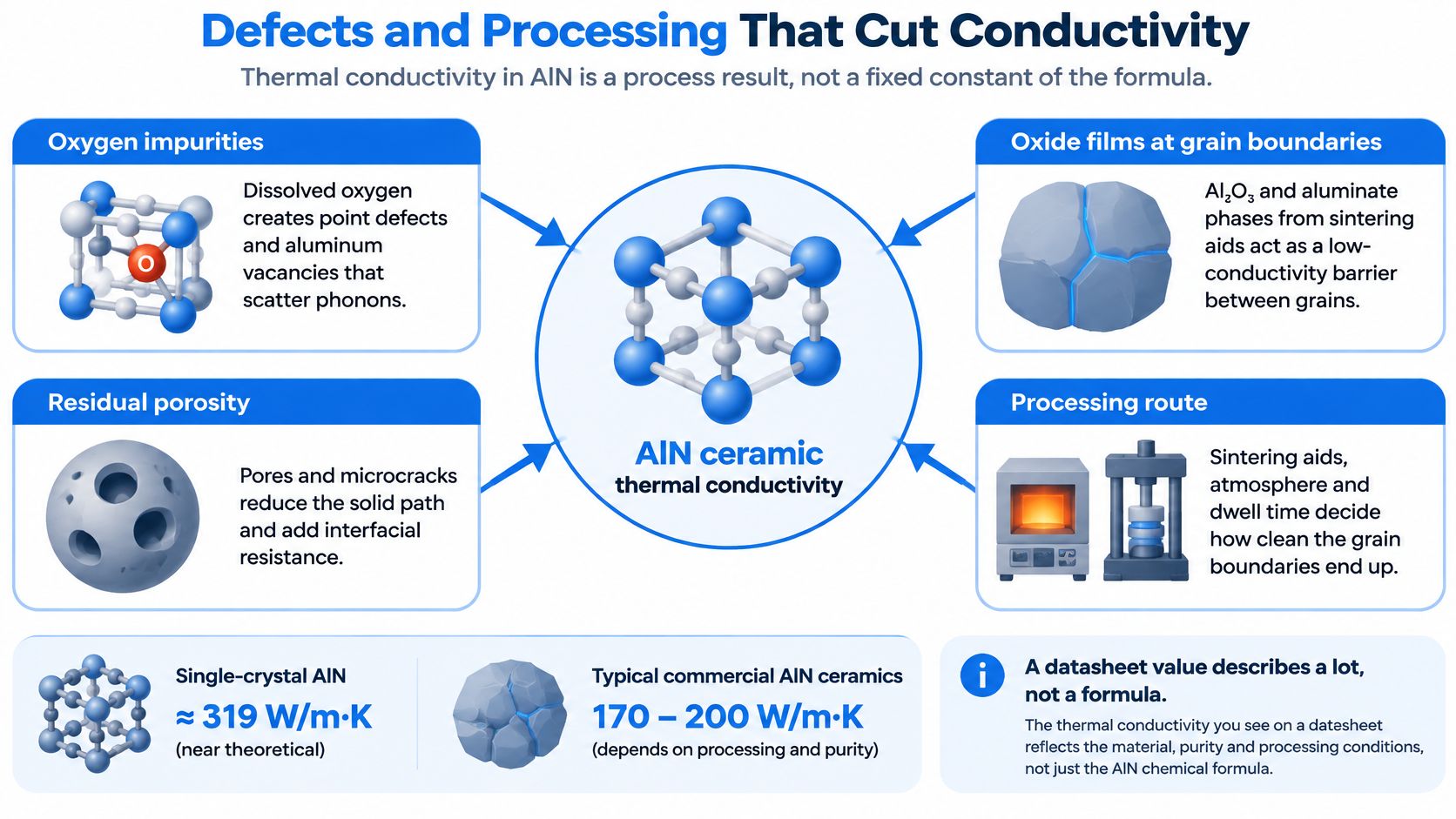
AlN thermal conductivity is a processing outcome, not a fixed consequence of the chemical formula. A manufacturer can produce the right compound while leaving a microstructure that interrupts heat transport.
Dissolved oxygen can create point defects and associated aluminum vacancies. Grain-boundary phases introduce additional interruptions between crystals, while pores remove solid material from the conduction path. Dislocations and damaged regions also disturb the ordered lattice through which heat travels.
The principal mechanisms are summarized visually below.
<a id="film-structure-can-outweigh-the-material-label"></a>
Film structure can outweigh the material label
The 2025 AlN film study published in Ceramics International reports 9.7 W/m·K for a weakly oriented ALD film, 26.5 W/m·K for reactive-sputtered material, and 190.6 W/m·K for strongly oriented MOVPE AlN, with the higher value associated with stronger c-axis orientation, larger grains, and fewer point defects. The same study reports thermal boundary conductance of 147 MW/m²·K, a separate interface property rather than another bulk conductivity value.
That spread is especially important for advanced packaging. A deposited thermal layer may have the correct composition but insufficient structural order to deliver the performance expected from a bulk ceramic. Deposition method is therefore useful information, but the resulting orientation, grain structure, and defect concentration are what explain the heat transport.
<a id="bulk-material-and-interfaces-need-different-properties"></a>
Bulk material and interfaces need different properties
Thermal conductivity describes transport through a material body. Thermal boundary conductance describes transfer across an interface. They have different units because they describe different physical restrictions.
A thin layer can have little geometric thickness and still introduce a consequential boundary resistance. Treating its interface as perfectly bonded in a simulation can therefore hide a limitation that improving the surrounding ceramic won't solve.
- Cleaner lattice chemistry reduces scattering within grains.
- Controlled grain boundaries limit obstructive secondary phases between grains.
- Higher density preserves a more continuous solid conduction path.
- Better structural orientation can improve transport in the direction relevant to a film.
These are process levers, not independent promises. Changing a sintering additive or deposition condition may improve one characteristic while altering another, so the finished material still needs a measured property basis.
AlN isn't inherently a high-conductivity substrate grade. Particular manufacturing routes and microstructures produce that performance.
This distinction becomes more consequential in buried thermal layers and heterogeneous integration, where a small region with poor transport can sit directly beneath a concentrated heat source.
<a id="how-temperature-and-thickness-change-the-result"></a>
How Temperature and Thickness Change the Result
A room-temperature conductivity value isn't automatically the value at the device's operating temperature. The crystalline AlN measurements cataloged by OSTI give 674 ± 56 W/m·K at 100 K, 237 ± 6 W/m·K near room temperature, and 186 ± 7 W/m·K at 400 K, approximately a 72% reduction between the coldest and hottest points.
| Temperature | Thermal conductivity | What it means for design | |---|---|---| | 100 K | 674 ± 56 W/m·K | Cryogenic crystal behavior, not a typical board operating point | | Near room temperature | 237 ± 6 W/m·K | This particular crystal, not an ideal-material guarantee | | 400 K | 186 ± 7 W/m·K | Approximately 72% below this sample's 100 K value |
The room-temperature result isn't a contradiction of higher-quality crystal measurements. It belongs to a different specimen with its own defect structure. Comparing values without matching the specimen conditions confuses material potential with sample performance.
<a id="a-hotter-lattice-scatters-heat-differently"></a>
A hotter lattice scatters heat differently
As the lattice becomes hotter, increased phonon interactions interrupt heat transport. For thermal modeling, the practical consequence is straightforward: a constant room-temperature input can make a hot region look more conductive than it is.
Use a conductivity-versus-temperature curve when it's available for the selected grade. If the documentation gives only a room-temperature point, identify that limitation in the model rather than extending the value across the operating range.
<a id="thin-material-can-change-conductivity-itself"></a>
Thin material can change conductivity itself
Thickness has a second meaning beyond the distance heat must cross. The same OSTI record describes a finding that phonons with mean free paths longer than approximately 0.7 micrometers contribute half of bulk AlN's room-temperature heat conduction, and a calculation predicting 348 W/m·K for pure nitrogen-14 AlN.
Long-traveling phonons can't contribute in the same way when they encounter a film boundary, small grain, or damaged region before completing that travel. This is why making an AlN layer thinner doesn't always preserve its bulk conductivity.
Keep these effects separate:
- Geometric thickness changes the distance heat must travel through a sheet.
- Boundary-limited transport can change the conductivity of the material itself.
- Temperature dependence changes the property at the operating point.
- Isotopic composition affects the intrinsic transport limit through atomic mass disorder.
For a conventional substrate, reducing thickness may help the thermal path, subject to electrical and mechanical requirements. For a very thin deposited layer, however, a bulk-property assumption needs additional justification. Record conductivity alongside temperature, thickness, orientation, impurity basis, and measurement method, so the model input describes an actual material condition.
<a id="from-bulk-aln-to-a-ceramic-pcb-thermal-path"></a>
From Bulk AlN to a Ceramic PCB Thermal Path
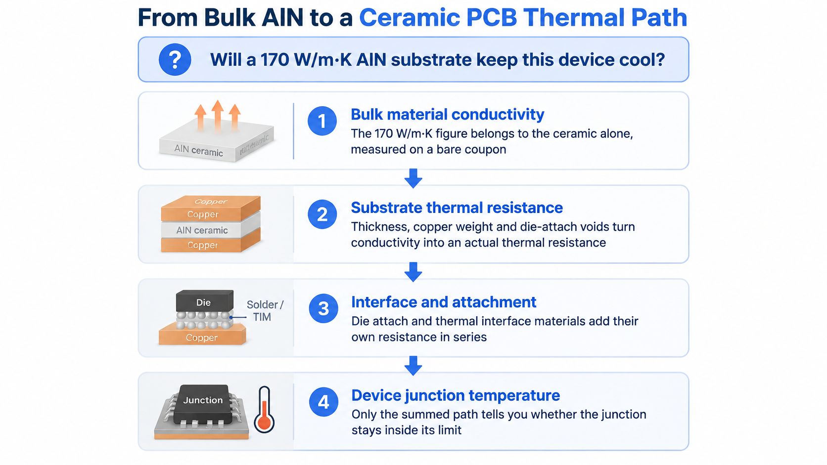
Will an AlN substrate keep a particular device cool? Conductivity alone can't answer that question. The AlN ceramic PCB guide from Hilelectronic describes published substrate values spanning approximately 150–240 W/m·K, while emphasizing that die attach, copper spreading, ceramic thickness, voids, metallization, and heatsink contact determine the completed assembly's thermal behavior.
Separate bulk conductivity, substrate thermal resistance, and junction-to-case thermal resistance before comparing boards. They aren't alternative names for the same specification.
The diagram below separates the material property from the assembled thermal result.
<a id="translate-the-sheet-into-resistance"></a>
Translate the sheet into resistance
For uniform, through-thickness conduction, the ceramic contribution can be screened with:
R = t / (k × A)
Here, t is ceramic thickness, k is conductivity, and A is the heat-transfer area. This relationship doesn't include lateral spreading, nonuniform heat flux, or contact resistance.
The distinction resolves a common purchasing mistake. A higher-conductivity ceramic doesn't necessarily have lower sheet resistance if it's also thicker. Nor does a low sheet resistance establish the temperature drop through the attachment layers.
For an LED module, compare complete candidate stacks under the same dissipated power and cooling boundary. A dense, thinner substrate with a well-controlled attach can outperform a nominally better ceramic grade paired with a thicker plate or a voided joint. The comparison must include the geometry, not just the catalog property.
<a id="walk-from-the-die-to-the-cooler"></a>
Walk from the die to the cooler
A useful thermal model follows the physical assembly: die, attachment, conductor spreading region, ceramic, backside attachment or interface, and cooling surface. The exact order depends on the construction, so draw the actual cross-section rather than borrowing a generic package stack.
- Die attachment needs realistic bond-line thickness and void assumptions.
- Copper and metallization need their actual geometry because heat spreads laterally.
- Ceramic needs grade-specific properties and finished thickness.
- Heatsink contact needs a defined interface material, contact area, and assembly condition.
For an RF or automotive module, thermal adequacy is only part of acceptance. The structure must also satisfy its insulation, circuit, and environmental requirements. Reviewing ceramic PCB construction alongside the thermal model helps keep those constraints connected.
The accompanying video provides another view of the board-level context.
<iframe width="100%" style="aspect-ratio: 16 / 9;" src="https://www.youtube.com/embed/ASE90dYZHKc" frameborder="0" allow="autoplay; encrypted-media" allowfullscreen></iframe>Keep the thermal boundary explicit. Junction-to-case stops at the defined case surface; a path extending through the heatsink and into ambient requires additional resistance terms.
Acceptance habit: Verify the assembled path under defined conditions. A bare-ceramic property certificate can't establish the finished device's junction temperature.
<a id="what-to-require-on-an-aln-substrate-datasheet"></a>
What to Require on an AlN Substrate Datasheet
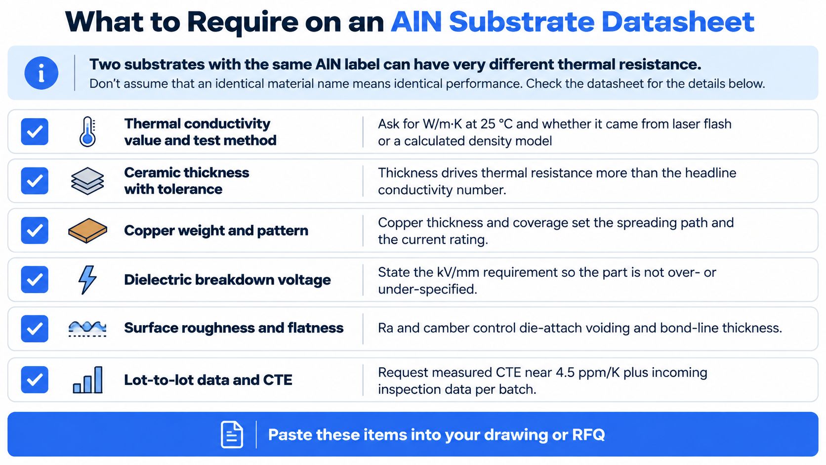
Two substrates with the same AlN designation can have different thermal resistance. Procurement needs a grade-specific, testable requirement, not an unqualified family-level property.
The Journal of Materials Science Materials in Electronics article on AlN processing describes pressureless-sintered polycrystalline grades as commonly below 200 W/m·K, while controlled lattice oxygen, near-full density, and limited secondary phases can support approximately 180 W/m·K or higher. That's a processing-dependent substrate expectation, not permission to assign an intrinsic crystal value to a finished board.
<a id="put-these-fields-in-the-drawing-or-rfq"></a>
Put these fields in the drawing or RFQ
- Test temperature, because the reported property must match the model's temperature basis.
- Material form and finished thickness, because a bulk ceramic and a deposited film aren't equivalent specimens.
- Density and residual porosity, because voids interrupt the solid conduction path.
- Oxygen content or a defined purity grade, because nominal AlN composition doesn't describe lattice defects.
- Sintering additives and secondary-phase controls, because grain-boundary chemistry affects transport.
- Crystal orientation where relevant, because textured materials need direction-specific interpretation.
- Measurement method and specimen direction, because in-plane and through-plane results aren't automatically interchangeable.
- Lot-level evidence, because a catalog typical doesn't establish an incoming batch's acceptance.
The checklist graphic can support a broader fabrication discussion; the written drawing should define the actual acceptance requirements.
<a id="define-what-passing-means"></a>
Define what passing means
State whether conductivity is a guaranteed minimum, a typical value, or a characterization result. Those categories have different procurement implications. A typical value may support early screening, but it shouldn't become the acceptance limit for a critical thermal path.
Also establish whether the evidence applies to starting ceramic, a representative coupon, or the finished substrate. Metallization and subsequent processing can change the part being evaluated, so traceability between the certificate and purchased construction matters.
For incoming acceptance, record the grade, lot identity, finished thickness, and agreed test basis together. If the thermal model depends on a particular property, document how that property will be supported during production rather than leaving it as an assumption.
Specify the test, not the trademark.
A complete specification doesn't need every possible material property. It needs the properties that control the design, the conditions under which they apply, and a practical way to verify them.
<a id="choose-aln-when-insulation-and-heat-must-share-one-board"></a>
Choose AlN When Insulation and Heat Must Share One Board
Choose AlN when the circuit needs electrical isolation and the ceramic is a meaningful thermal bottleneck. Power modules, dense LED engines, and thermally demanding RF assemblies are sensible candidates. The decision is strongest when improving the substrate changes the predicted junction temperature without compromising the electrical or mechanical design.
Stay with alumina when its selected grade satisfies the thermal requirement. A material upgrade isn't useful merely because it raises the conductivity on a drawing. If the limiting resistance is elsewhere, improving the attachment, spreading area, or cooler may be the more effective change.
<a id="match-the-construction-to-the-constraint"></a>
Match the construction to the constraint
A metal-core board is another option when the circuit can accept a metal base with an appropriate insulating structure. For LED and general thermal layouts, assess metal-core PCB construction alongside ceramic rather than assuming every hot board needs AlN.
Use different decision tests for each candidate:
- AlN ceramic fits when insulation and heat transfer must coexist through the substrate.
- Alumina ceramic fits when its thermal performance meets the requirement without an AlN upgrade.
- Metal-core construction fits when the circuit architecture allows a metal-backed thermal path and the dielectric structure meets the electrical requirement.
These aren't rankings from best to worst. They're different ways to satisfy a package's heat-flow and isolation constraints.
<a id="prepare-a-fabrication-ready-thermal-brief"></a>
Prepare a fabrication-ready thermal brief
At Lianyuhong Technology Co.,Ltd, we fabricate ceramic PCBs using Al2O3, AlN, and BeO substrates with direct-bonded copper and thick-film technology, supporting up to 12 oz copper for high-power, high-temperature, and thermal-management applications. The material and conductor construction should be chosen together, not as separate late-stage substitutions.
For engineering review, include the Gerbers, stack-up, ceramic thickness, dissipated power, target junction temperature, and cooling conditions. Attach the conductivity test basis and identify which thermal interfaces are fixed and which can still change.
That package makes the design question concrete: which manufacturable construction satisfies the device limit with an acceptable electrical and mechanical margin? Judge the board by the complete thermal path, not by the most impressive crystal result.
Lianyuhong Technology Co.,Ltd offers ceramic PCB fabrication with DBC and thick-film options, alongside metal-core boards for thermal-management designs. Visit Lianyuhong Technology Co.,Ltd and send your Gerbers, stack-up, target junction temperature, ceramic thickness, and conductivity test conditions for a DFM review of the appropriate board construction.