
Your team has finished the schematic, placed the major components, and started routing. Then the RF designer finds that the radio path loses too much energy on standard FR-4, while the power engineer flags an LED driver that runs hot inside its enclosure. The circuit works on paper, but the proposed board construction doesn't meet the product's physical requirements.
That's when PCB manufacturing techniques become engineering decisions rather than purchasing options. Adding layers can solve routing congestion, but it won't automatically fix dielectric loss. A metal base can improve heat transfer, but it won't replace a properly designed heatsink. Laser microvias can free routing space, but they also introduce fabrication and qualification requirements.
The right starting point is the constraint you can't relax: board area, operating temperature, bend geometry, transmission loss, signal speed, or assembly yield. Cost matters throughout, but comparing bare-board prices before resolving those constraints often leads to the wrong construction.
Rigid multilayer fabrication handles conventional routing and power distribution. HDI addresses density, flex and rigid-flex address movement and packaging, and metal-core or ceramic substrates address different thermal problems. Low-loss laminates support RF paths, backdrilling removes troublesome via stubs, and controlled SMT printing and reflow turn a manufacturable board into a reliable assembly. These techniques aren't mutually exclusive. A product may need several, but each should solve a specific problem.
Table of Contents
- 1. Rigid Multilayer PCB Fabrication (Subtractive Etch and Lamination)
- 2. High-Density Interconnect (HDI) with Laser Microvias
- 3. Flexible and Rigid-Flex PCB Fabrication
- 4. Metal Core PCB (MCPCB) for Thermal Management
- 5. High-Frequency PCB Using PTFE and Hydrocarbon Laminates
- 6. Ceramic PCB Substrates (DBC and Thick-Film)
- 7. Backdrilling for Signal Integrity in High-Speed Boards
- 8. SMT Stencil Printing and Reflow Assembly
- How the 8 PCB Manufacturing Techniques Compare at a Glance
- Choosing the Right PCB Manufacturing Technique for Your Design
<a id="1-rigid-multilayer-pcb-fabrication-subtractive-etch-and-lamination"></a>
1. Rigid Multilayer PCB Fabrication (Subtractive Etch and Lamination)
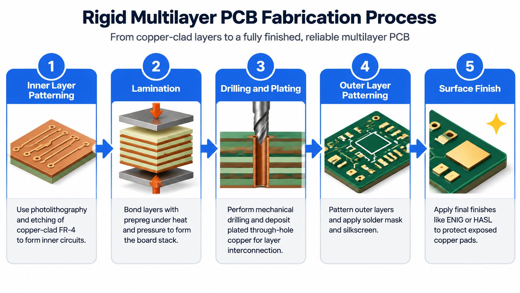
Start with rigid multilayer FR-4 when routing, power distribution, and mechanical support are the main requirements. Industrial controllers, computing boards, and networking switches commonly fit this construction because designers can separate signal routing from reference and power planes.
The fabricator images a resist onto copper-clad laminate, etches away exposed copper, and bonds the patterned inner layers with dielectric prepreg. Drilling and copper plating connect the layers, followed by outer-layer patterning, solder mask, surface finish, marking, and electrical testing. ALLPCB's manufacturing history describes this imaging, etching, lamination, and plated-interconnect foundation.
<a id="make-the-stack-up-part-of-the-design"></a>
Make the Stack-Up Part of the Design
For an industrial controller with a processor, motor interfaces, and communications ports, dedicate continuous reference planes beneath critical signals. Don't add layers merely because the initial placement is difficult to route. Revisit connector positions, component orientation, and power distribution before committing to a more complicated stack.
- Balance the construction: Keep dielectric thicknesses and copper distribution reasonably symmetrical to reduce warpage risk.
- Define electrical requirements: Document impedance targets, reference layers, and finished copper requirements before freezing trace geometry.
- Match the thermal exposure: Select laminate properties for assembly temperatures, operating conditions, and anticipated rework.
- Close the manufacturing gaps: Resolve drill sizes, annular rings, copper clearances, and solder-mask features during DFM review.
Choose this when a rigid board can meet the product's density, thermal, and electrical requirements using conventional drilled interconnects.
Avoid this when the design needs repeated bending, exceptionally compact package escape, or a thermal path that ordinary laminate construction can't provide. Adding layers won't remove those limitations.
<a id="2-high-density-interconnect-hdi-with-laser-microvias"></a>
2. High-Density Interconnect (HDI) with Laser Microvias
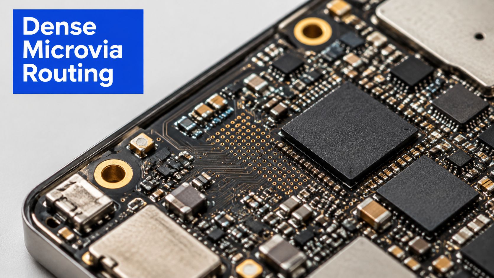
A compact camera module can have enough total board area yet still lack room to escape its processor package. HDI solves local interconnection density, using laser-drilled microvias and sequential build-up layers rather than forcing every connection through the full board thickness.
Its adoption reflects that practical need. IPC's PCB Technology Trends study reported that the share of surveyed manufacturers using or fabricating HDI increased from 37.5% to slightly above 49% over the preceding five years, as summarized in Viasion's manufacturing outlook.
<a id="qualify-the-interconnect-not-just-the-trace-width"></a>
Qualify the Interconnect, Not Just the Trace Width
Smartphones, wearables, and compact processor modules benefit when microvias release routing channels beneath dense packages. The trade-off is additional lamination, registration, filling, and plating control. An any-layer construction isn't automatically the best answer because it offers the most routing freedom.
Practical rule: Use the least complicated build-up structure that successfully escapes the package and preserves the required reference planes.
Plan the BGA escape before completing placement. Define filled and capped via-in-pad features wherever open holes would otherwise draw solder away from component joints.
- Check reliability evidence: Review microvia cross-sections and relevant thermal-cycling qualification.
- Define the geometry: Agree on capture pads, dielectric thickness, via arrangement, and registration allowances.
- Control complexity: Compare staggered and stacked structures before selecting the denser option.
Choose this when package escape or enclosure size makes conventional through-via routing impractical.
Avoid this when a placement change or conventional multilayer stack meets the same requirement. HDI adds value when it removes a demonstrated constraint, not when it merely produces a smaller capability figure on a drawing.
<a id="3-flexible-and-rigid-flex-pcb-fabrication"></a>
3. Flexible and Rigid-Flex PCB Fabrication
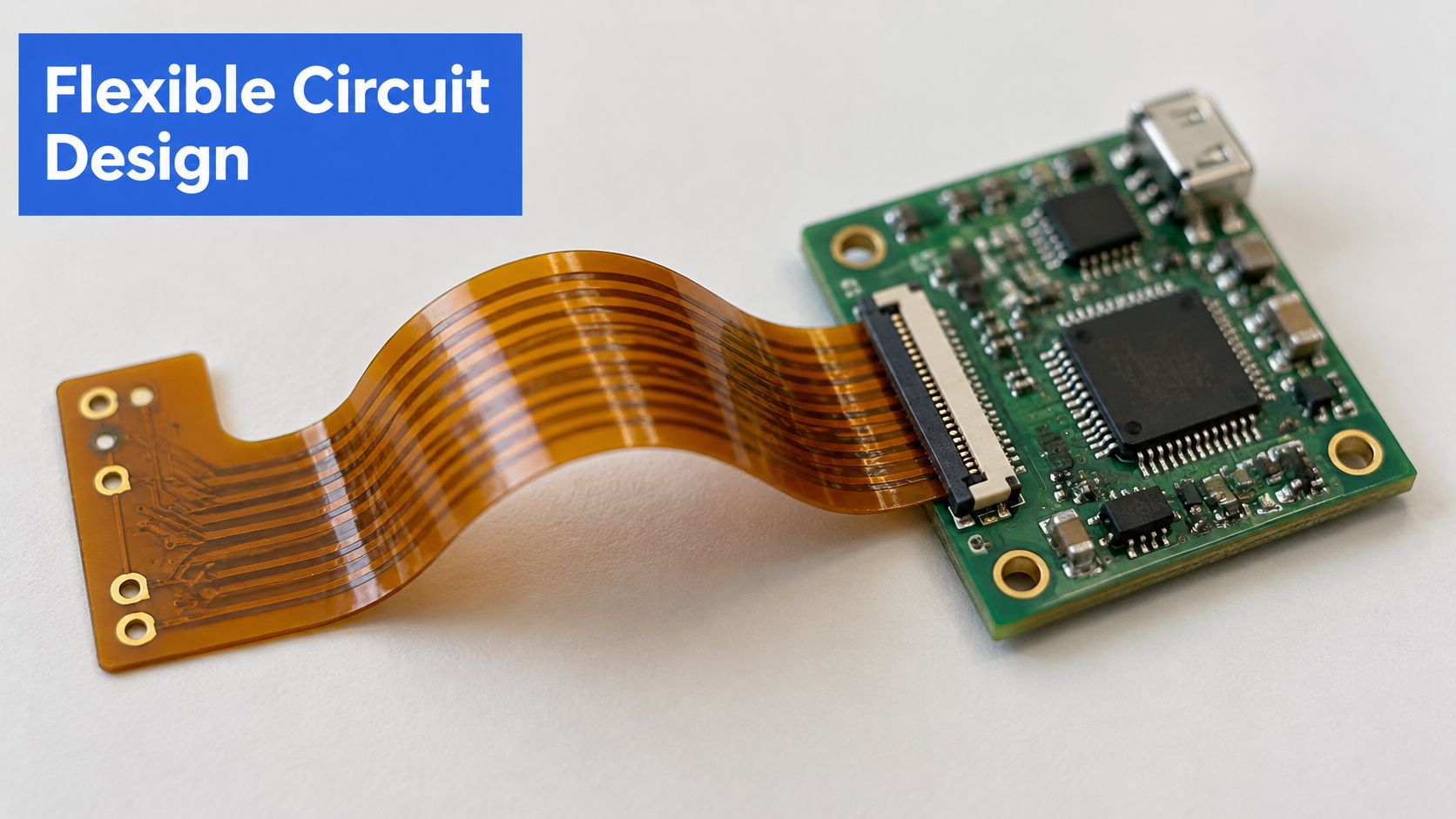
A circuit that must fold into an enclosure needs a mechanical design, not just a flexible material. Flexible PCBs use copper conductors on bendable dielectrics, commonly polyimide. Rigid-flex combines flexible interconnections with rigid component-mounting regions.
Consider a medical imaging probe with electronics distributed through a narrow housing. A rigid-flex assembly can connect those regions without separate cable connectors, but the flexible sections still need controlled bends, assembly access, and protection from abrasion.
<a id="separate-installation-bends-from-repeated-movement"></a>
Separate Installation Bends from Repeated Movement
A camera ribbon folded during installation faces a different duty from a hinge interconnect that moves throughout service. Define that distinction before selecting copper construction, stack-up, and protective layers.
For dynamic bending, rolled-annealed copper is a useful starting choice, but it doesn't excuse poor routing. Route conductors across the bend axis, use smooth transitions, and keep vias, solder joints, and abrupt width changes away from active bending regions.
- Document the mechanics: Show bend locations, permitted radii, movement direction, and stiffener positions.
- Control transitions: Protect the boundary between rigid and flexible regions from concentrated strain.
- Specify protective features: Include coverlay openings, stiffener materials, and connector contact details.
The rigid-flex PCB design guidelines provide a useful framework for coordinating these mechanical and fabrication requirements before layout release.
Choose this when folding, movement, weight, or connector removal justifies an integrated flexible interconnect.
Avoid this when a replaceable cable assembly meets the packaging requirement and makes service easier. Rigid-flex can reduce connection points, but replacing a damaged integrated assembly may be more expensive than replacing a separate cable. Compare the complete assembly and repair strategy, not just the board outline.
<a id="4-metal-core-pcb-mcpcb-for-thermal-management"></a>
4. Metal Core PCB (MCPCB) for Thermal Management
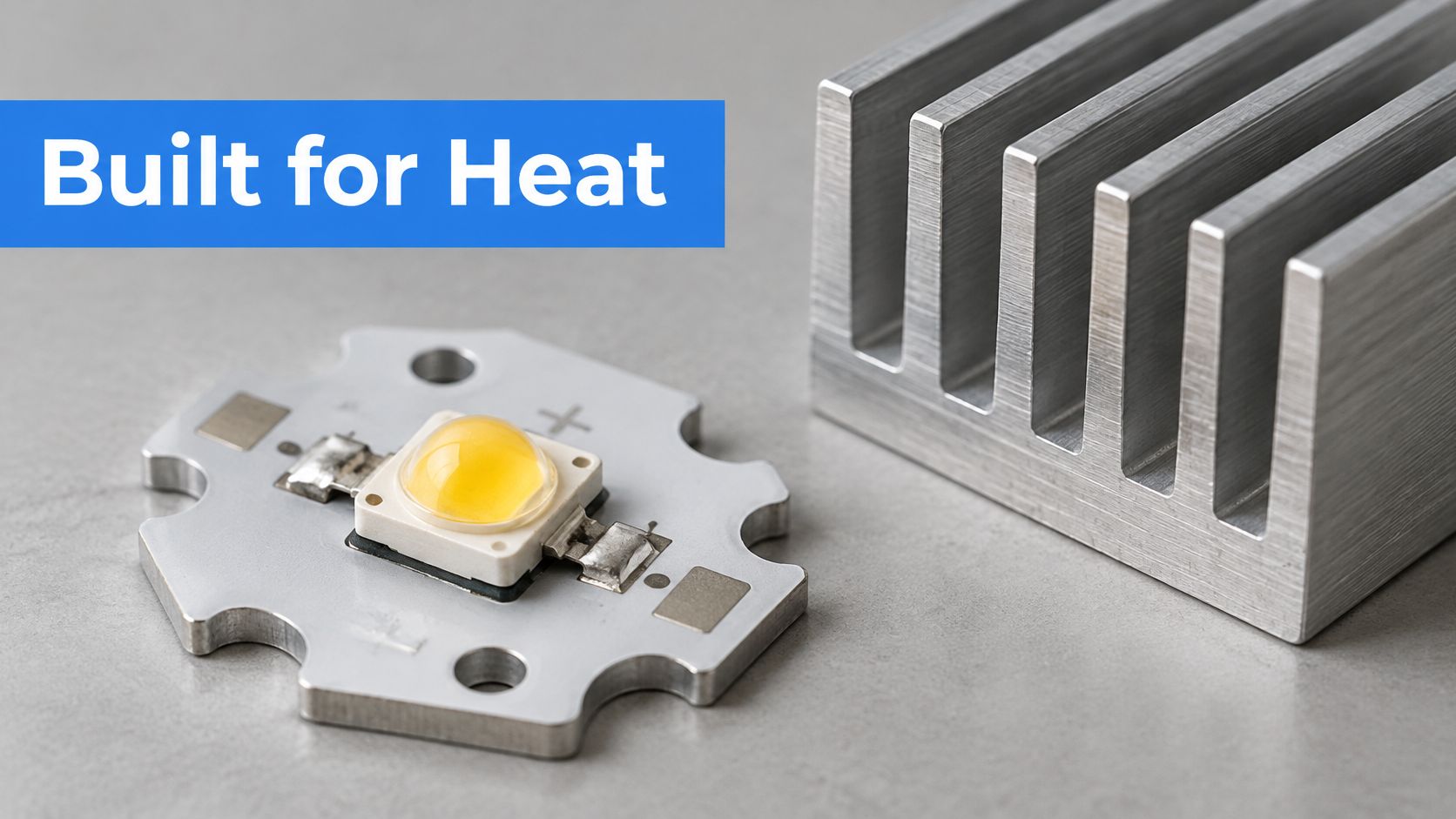
An LED streetlight can have generous copper traces and still overheat because heat must cross an unsuitable dielectric before reaching the housing. Metal-core construction addresses that heat-transfer path, typically combining a copper circuit layer, an electrically insulating thermal dielectric, and an aluminum or copper base.
The metal spreads heat toward a heatsink or chassis. It doesn't make the heat disappear, and it doesn't compensate for poor contact between the board and its mounting surface.
<a id="design-the-complete-thermal-path"></a>
Design the Complete Thermal Path
For an automotive headlamp module, follow heat from the LED junction through the package, solder joint, board dielectric, metal base, interface material, and housing. Improving the metal base alone may deliver little benefit if another interface dominates thermal resistance.
- Select the dielectric deliberately: Balance thermal conductivity, thickness, electrical isolation, and manufacturing requirements.
- Size conductors for current: A metal base doesn't prevent narrow copper traces from producing localized heating.
- Define the mounting interface: Specify flatness, thermal interface material, fastener locations, and assembly pressure.
- Check hole isolation: Don't copy plated-hole or thermal-via details from FR-4 without confirming the metal-core construction.
A metal-core board is part of the heatsink assembly. Validate it in the intended housing, not only on an open laboratory bench.
Choose this when concentrated heat from LEDs or power components needs a direct path into a chassis or heatsink.
Avoid this when the true limitation is inadequate external cooling or when dense multilayer routing dominates the design. MCPCB construction can constrain routing and interconnect options. A separate power substrate connected to a conventional control board may provide a cleaner solution than forcing every circuit onto the same metal base.
<a id="5-high-frequency-pcb-using-ptfe-and-hydrocarbon-laminates"></a>
5. High-Frequency PCB Using PTFE and Hydrocarbon Laminates
RF loss is a material-and-geometry problem, not an impedance problem. A trace can have the correct characteristic impedance while still losing too much energy along its length.
PTFE-based and hydrocarbon-ceramic laminates provide alternatives to standard FR-4 when dielectric loss and material stability matter. Rogers RO4000-series materials, PTFE constructions, and suitable Taconic laminates are relevant choices for antenna feeds, microwave instruments, radar modules, and satellite terminals.
<a id="spend-on-the-rf-path-not-automatically-on-every-layer"></a>
Spend on the RF Path, Not Automatically on Every Layer
Say a communications board combines an antenna feed network with a digital controller. A hybrid stack-up can place RF circuitry on a suitable low-loss laminate while retaining FR-4 elsewhere. That approach requires compatible bonding materials and a fabrication plan that accounts for different material behavior.
Don't select by brand name alone. Use the specific laminate grade, construction, and supplier material properties in the transmission-line model.
- Model the operating conditions: Use dielectric constant and dissipation factor appropriate to the frequency and construction.
- Include conductor effects: Copper roughness, trace geometry, and etch compensation influence transmission loss.
- Specify meaningful verification: Use TDR for impedance and suitable VNA measurements for insertion loss.
- Review hybrid interfaces: Confirm bonding, registration, drilling, and plated-interconnect requirements.
The Rogers PCB manufacturer guide helps frame material and fabrication discussions around the actual RF requirements rather than a generic low-loss label.
Choose this when a modeled or measured RF path cannot meet its loss, stability, or impedance requirements on the proposed conventional laminate.
Avoid this when short traces on an appropriate FR-4 construction already satisfy the electrical budget. Conversely, don't retain FR-4 solely to reduce material cost if the resulting loss requires more amplifier power or prevents the product from meeting its specification.
<a id="6-ceramic-pcb-substrates-dbc-and-thick-film"></a>
6. Ceramic PCB Substrates (DBC and Thick-Film)
Metal-core boards and ceramic substrates solve different power-packaging problems. Ceramic becomes relevant when heat transfer, electrical insulation, and operating conditions must be addressed together, especially near power semiconductor dies.
Direct bonded copper, or DBC, joins copper foil to a ceramic substrate. Thick-film processing instead prints and fires conductive pastes onto ceramic. These aren't interchangeable routes: conductor properties, feature geometry, attachment methods, and production economics differ.
<a id="match-the-ceramic-to-the-power-assembly"></a>
Match the Ceramic to the Power Assembly
An electric-vehicle traction inverter using SiC switches needs coordinated decisions about substrate material, copper pattern, die attach, electrical clearances, and cooling. Selecting the ceramic after completing the power layout leaves too many coupled decisions unresolved.
Alumina is a practical option where it meets the thermal requirement. Aluminum nitride is worth considering when substrate thermal resistance is the binding constraint and the budget supports it. Neither choice eliminates stresses caused by different expansion behavior across copper, ceramic, attachment layers, and the cooling structure.
- Shape copper for reliability: Use rounded transitions and avoid concentrated mechanical stress.
- Define attachment early: Coordinate solder or sintered-silver die attach with metallization and subsequent assembly.
- Specify the conductor: Match copper thickness and pattern tolerances to electrical and mechanical needs.
- Protect the substrate: Account for ceramic brittleness during fastening, handling, and assembly.
Engineering judgement: Select ceramic as part of a power-module architecture, not as an expensive replacement for an otherwise adequate control board.
Choose this when power modules, laser diode drivers, or demanding amplifier assemblies require the combined thermal and insulating properties.
Avoid this when FR-4 with appropriate cooling, or an insulated metal substrate, meets the requirements. Ceramic adds handling and attachment challenges, and it doesn't provide the routing flexibility of a conventional multilayer logic board.
<a id="7-backdrilling-for-signal-integrity-in-high-speed-boards"></a>
7. Backdrilling for Signal Integrity in High-Speed Boards
A plated through-via can connect a surface trace to an internal signal layer while leaving an unused barrel beneath that connection. That unused section is a via stub, and its electrical behavior can disturb a high-speed channel.
Backdrilling removes the unwanted barrel with a larger, controlled-depth drill. It modifies an existing rigid-board construction rather than replacing its laminate or interconnect architecture.
<a id="remove-the-stub-only-where-it-matters"></a>
Remove the Stub Only Where It Matters
Consider a router line card with differential channels passing through a thick board. The active connection may use only part of each via, leaving a substantial unused section. Simulate the channel with realistic via geometry before assigning backdrilling across the design.
The manufacturing precision behind such interconnect choices has changed considerably. An IPC manufacturing report describes via diameters shrinking from approximately 0.25 inches to 20 micrometers over approximately the preceding fifty years, although those figures span different interconnect technologies rather than defining a backdrilling capability.
For backdrilling, depth control and layer registration matter more than an impressive minimum-hole specification.
- Identify affected nets: Use channel analysis to locate stubs that materially affect insertion or return loss.
- Document each operation: State the entry side, stop layer, drill requirements, and protected copper.
- Allow for residual stub: Include manufacturing tolerance in the electrical model rather than assuming perfect removal.
- Verify production geometry: Use appropriate cross-section or inspection coupons to check the resulting construction.
Choose this when unused through-via barrels prevent a high-speed channel from meeting its electrical budget.
Avoid this when the channel already passes, the via transition has another dominant problem, or the layer arrangement leaves little useful stub to remove. Backdrilling can't repair poor reference-plane transitions, excessive trace loss, or unsuitable connector launches. Model the complete channel before paying for selective mechanical removal.
<a id="8-smt-stencil-printing-and-reflow-assembly"></a>
8. SMT Stencil Printing and Reflow Assembly
A well-fabricated bare board can still fail during assembly. SMT begins with stencil printing of solder paste, followed by component placement and controlled reflow. Paste volume, alignment, release behavior, and thermal balance all affect the resulting joints.
Published manufacturing work estimates that approximately 50%–70% of assembly defects originate during solder-paste printing, according to the manufacturing study published by Springer. That makes printing a process to control, not merely a step to inspect afterward.
<a id="control-deposits-before-placing-components"></a>
Control Deposits Before Placing Components
For an IoT module containing QFN packages, hidden thermal pads, and small passives, one stencil design must accommodate very different solder-volume requirements. Aperture shape, stencil thickness, surface treatment, paste condition, and board support need coordinated decisions.
Use the PCB stencil manufacturer guide to connect aperture design with paste release and component requirements.
- Measure the print: Use SPI to track deposit volume, height, area, and offset.
- Respond to trends: Correlate printing excursions with cleaning, paste age, support, and printing settings.
- Profile the assembly: Measure temperatures at thermally different locations instead of copying another board's oven recipe.
- Inspect hidden joints: Combine AOI with appropriate X-ray inspection and electrical or functional testing.
The assembly sequence is shown below.
<iframe width="100%" style="aspect-ratio: 16 / 9;" src="https://www.youtube.com/embed/cEQpg7kOp9A" frameborder="0" allow="autoplay; encrypted-media" allowfullscreen></iframe>Choose this when surface-mount components and repeatable automated assembly suit the product.
Avoid this when treating reflow as the only attachment process would compromise mechanically loaded connectors or unsuitable power parts. Mixed SMT and through-hole assembly is often the correct answer. Don't expect post-reflow inspection to compensate for unstable printing or an unverified thermal profile.
<a id="how-the-8-pcb-manufacturing-techniques-compare-at-a-glance"></a>
How the 8 PCB Manufacturing Techniques Compare at a Glance
| Item | Primary Benefit | Main Trade-Off | Typical Applications | |---|---|---|---| | Rigid Multilayer PCB Fabrication (Subtractive Etch and Lamination) | Mature, cost-effective fabrication with broad material and assembly compatibility | Through-hole vias limit routing density and high-frequency performance | Consumer electronics, industrial control, networking, computing | | High-Density Interconnect (HDI) with Laser Microvias | High routing density in compact boards with improved signal integrity | Higher cost and process complexity than standard multilayer boards | Smartphones, wearables, medical devices, compact IoT modules | | Flexible and Rigid-Flex PCB Fabrication | Reduces cables, weight, and volume while enabling flexible form factors | Higher cost and design care needed to prevent bend-area damage | Foldable devices, wearables, medical devices, automotive interiors | | Metal Core PCB (MCPCB) for Thermal Management | Efficiently spreads heat from high-power components | Limited routing complexity and heavier than FR-4 | LED and automotive lighting, power electronics, motor drives | | High-Frequency PCB Using PTFE and Hydrocarbon Laminates | Low signal loss and stable electrical performance at high frequencies | Costlier materials and more demanding fabrication | Automotive radar, 5G infrastructure, satellite communications, microwave equipment | | Ceramic PCB Substrates (DBC and Thick-Film) | Excellent thermal conductivity and reliability at high temperatures | High cost, brittleness, and limited routing density | EV traction inverters, industrial power modules, high-power RF, laser drivers | | Backdrilling for Signal Integrity in High-Speed Boards | Removes via stubs to reduce reflections and improve high-speed signal quality | Adds fabrication cost and requires precise depth control | Telecom backplanes, data center switches, high-speed servers, test equipment | | SMT Stencil Printing and Reflow Assembly | Enables automated, high-throughput assembly of dense, fine-pitch components | Requires careful stencil and thermal-profile control; hidden joints need inspection | Consumer electronics, automotive ECUs, IoT modules, industrial controls |
<a id="choosing-the-right-pcb-manufacturing-technique-for-your-design"></a>
Choosing the Right PCB Manufacturing Technique for Your Design
Start with the binding constraint, then select the simplest construction that satisfies it. Conventional rigid multilayer fabrication remains the sensible baseline when it meets routing, thermal, mechanical, and electrical needs. Add HDI for a demonstrated density problem, flex for a defined mechanical requirement, and specialized substrates for a quantified thermal or RF limitation.
Keep related decisions separate. Low-loss laminate addresses dielectric performance, while backdrilling addresses unused via barrels. Metal-core construction improves a particular heat path, while ceramic belongs within a broader power-module architecture. SMT process controls address assembly risk regardless of which bare-board technology you select.
<a id="compare-the-finished-product-not-just-the-board-quote"></a>
Compare the Finished Product, Not Just the Board Quote
Evaluate fabrication cost alongside assembly yield, cooling hardware, test coverage, repair access, and service life. A cheaper board isn't cheaper if it requires an additional connector, a larger heatsink, or repeated rework.
Environmental comparisons need the same discipline. The sustainability review in Environmental Research Communications identifies PCB production as energy- and chemically intensive and explains the limitations of inconsistent life-cycle information. Compare alternatives using the same assessment boundary, including relevant electricity, chemicals, water, scrap, transport, and recovery assumptions.
Repairability also belongs in the layout discussion. Provide access to likely service components, use removable connections where appropriate, and avoid making a small replaceable section inseparable from an expensive assembly.
Promising recovery chemistry isn't a substitute for production qualification or a practical collection and disassembly process.
The University of Maryland's DissolvPCB project reported more than 98% material recovery in initial testing, while noting that assembly, disassembly, and recycling still required manual effort. That's a development direction, not evidence that dissolvable substrates can replace qualified FR-4 across existing products.
Before release, prepare Gerber or ODB++ files, drill data, stack-up requirements, a BOM with manufacturer part numbers, and pick-and-place data. Include mechanical drawings, critical electrical requirements, and inspection expectations. Resolve DFM feedback before approving manufacture.
Lianyuhong Technology Co.,Ltd is a Shenzhen-based manufacturer and assembler offering these fabrication and assembly techniques under one quality system. Our secure upload process includes engineering review of each order for manufacturability and component availability, followed by a detailed quotation with lead-time options. Use that review to settle the construction and assembly plan before committing the design to production.
Lianyuhong Technology Co.,Ltd provides PCB fabrication, component sourcing, assembly, and testing for conventional and specialized board constructions. Visit Lianyuhong Technology Co.,Ltd to upload your Gerber or ODB++ files, BOM, and pick-and-place data through the secure portal, and request engineering DFM feedback before release.