
Your stencil quote has arrived, but it lists only a frame, a foil thickness and a finish. Your board combines a fine-pitch BGA, an RF shield and a power connector, and nobody has explained whether the proposed stencil can print all of them reliably.
That's the qualification problem. A PCB stencil manufacturer should do more than cut your paste layer into metal. The supplier should identify conflicting paste requirements, explain the proposed compromises and provide evidence you can check on the assembly line. Treat the stencil as a yield decision, not a catalogue item.
Table of Contents
- Spec Sheet to Send With Every Stencil Quote
- Mixed-Pitch Boards and When to Step the Stencil
- Laser-Cut Versus Electroformed Stencils
- Nano Coating Versus Electropolish for Your Finish
- Lead Times, MOQ and What Drives Stencil Pricing
- QA Evidence and a First-Article Stencil Test
- Send Your First Stencil RFQ With This Checklist
<a id="spec-sheet-to-send-with-every-stencil-quote"></a>
Spec Sheet to Send With Every Stencil Quote
A request that says only “stencil for my board” leaves the supplier to make decisions you haven't approved. If the foil suits the connectors but not the smallest BGA apertures, you may discover the mismatch only after printing starts.
The specification sheet is your first control point. Match the frame to your printer before discussing finishes, then define the component families that control thickness and paste volume.
Use the following table as an RFQ template. Numerical release guidelines and the fine-feature thickness window come from the EPC solder-stencil design guidance, which identifies approximately 50–75 µm for 01005 and 0.3 mm-pitch assemblies, an aspect ratio above 1.5, and an area ratio above 0.66.
| Specification | Typical Value | Why It Matters | |---|---|---| | Foil thickness, miniature and fine-pitch packages | Fine-feature window stated above, subject to DFM | Supports release from small apertures | | Foil thickness, general SMT and QFP | Supplier recommendation based on the component mix | Avoids selecting thickness from package labels alone | | Foil thickness, large pads and RF shields | Local paste-volume requirement to be confirmed | May require a step or local thickening | | Aspect ratio | Guideline stated above | Aperture width divided by foil thickness | | Area ratio | Guideline stated above | Aperture opening area divided by aperture-wall area | | Base material | State the stainless grade and condition | Tie the material certificate to the supplied foil | | Aperture tolerance | Supplier to state in writing | Define how dimensions are measured and sampled | | Frame size | Match the printer and mounting system | Prevents an equipment compatibility failure | | Fiducials and registration | Show on the approved drawing | Check alignment before cutting |
<a id="define-what-the-supplier-must-review"></a>
Define What the Supplier Must Review
Don't let a single “standard thickness” replace component-level DFM. Ask the engineer to classify apertures by pitch, pad geometry and required solder volume, then identify which family sets the limiting release condition.
The ratio definitions matter because reducing aperture size without reconsidering foil thickness can make release harder. Conversely, thinning the foil to help the smallest features can leave larger pads short of paste. Neither ratio proves that the whole board will assemble reliably.
Request a marked-up drawing showing reductions, rounded corners, segmented openings and proposed step regions. Approve those changes explicitly, rather than allowing undocumented edits between quotation and cutting.
RFQ rule: A tolerance without a measurement method and sampling plan isn't a complete acceptance requirement.
<a id="send-a-complete-file-package"></a>
Send a Complete File Package
Include the Gerber files, board revision, pad-to-aperture map or drawing, board thickness and component list. Add printer requirements, panel details and any known paste-volume concerns.
State whether you need a first-article review before releasing the stencil for routine production. The supplier should review the actual component mix before pricing, not discover the difficult apertures after you've placed the order.
<a id="mixed-pitch-boards-and-when-to-step-the-stencil"></a>
Mixed-Pitch Boards and When to Step the Stencil
Miniature components need reliable release from small openings, while shields, connectors and large thermal pads may need substantially more paste. Making the entire foil thinner or thicker shifts the problem rather than resolving it.
The conflict is explicit in IPC's work on mixed paste-height requirements: large features may require approximately 150 µm paste height. The same experimental work found that a 2 mil electroformed stencil provided higher transfer efficiency than a 3 mil version, while spacing between prints affected smearing in a two-print process.
<a id="compare-the-available-compromises"></a>
Compare the Available Compromises
| Approach | What It Protects | What Can Fail | |---|---|---| | One thin foil | Release on miniature apertures | Large features may receive insufficient paste | | One thick foil | Paste volume on larger features | Small apertures may release poorly or print excessive deposits | | Stepped stencil | Different local volume requirements | Step placement must fit the layout and printing process | | Two-print process | Separately controlled deposits | Print interaction and smearing require validation |
A uniform thin foil is reasonable only if the larger features still meet their assembly requirements. Don't approve it because the BGA prints cleanly while leaving the connector results unexamined.
A uniform thick foil has the opposite burden of proof. More theoretical volume doesn't help if paste remains inside the smallest apertures.
A stepped stencil addresses the conflict locally. Have the supplier mark the transition locations, keep-out requirements and inspection points on the drawing. If the layout doesn't leave room for workable transitions, moving to a stepped design on paper won't solve the production problem.
<a id="use-layout-freedom-before-adding-process-complexity"></a>
Use Layout Freedom Before Adding Process Complexity
Local thickening or a revised pad arrangement may be worth evaluating before committing to separate print operations. Treat these as engineering alternatives, not guaranteed cheaper fixes. Compare the stencil quotation with the added setup, inspection and handling required on the line.
Consider a hypothetical startup board containing a fine-pitch BGA, shielded RF can and power connector. If the thin-foil trial passes SPI at the BGA but leaves the shield deposits below their approved volume limits, that stencil hasn't passed the board.
The thinnest stencil isn't automatically the best stencil. Approve the full component mix, not the easiest inspection result.
Choose using paste measurements, post-reflow results and expected production volume. A more involved print process needs a repeatability case, not just a successful demonstration board.
<a id="laser-cut-versus-electroformed-stencils"></a>
Laser-Cut Versus Electroformed Stencils
The two processes build the foil differently, and that difference shows up at the aperture wall. Laser cutting starts with a solid stainless-steel sheet and removes material with a laser, leaving apertures with a slight taper and a cut edge whose smoothness depends on the machine and any post-cut finishing. Electroforming builds the foil the other way: nickel is deposited onto a mandrel until it reaches the target thickness, then the foil is separated, which produces apertures with very smooth, near-vertical walls.
Smooth walls matter when paste release is the limiting factor. Fine-pitch and low-area-ratio apertures are where the wall condition tends to decide whether a print passes or fails.
Ask the manufacturer to compare processes against your hardest aperture family, not against a general claim that one technology is superior. A process name doesn't establish the quality of the foil you'll receive. Laser-cut stainless steel is the established approach, and the history of solder-stencil manufacturing traces the progression from etched brass to laser cutting and finished foils. That history explains why laser cutting is familiar. It doesn't qualify a particular supplier.
<a id="compare-actual-outputs"></a>
Compare Actual Outputs
| Decision Point | Laser-Cut Proposal | Electroformed Proposal | |---|---|---| | Smallest aperture family | Request dimensions and wall inspection evidence | Request equivalent evidence for the proposed construction | | Mixed-volume board | Obtain the proposed local thickness solution | Confirm how the supplier would meet the same volume requirements | | Print qualification | Test with the intended paste | Use the same acceptance criteria | | Commercial comparison | Separate fabrication and finish costs | Include any process-specific engineering costs |
Electroforming typically costs more and can carry longer lead times, so treat it as a targeted option rather than a default upgrade. I've seen shops quote it across a whole stencil when only one connector footprint was causing release failures. Price it against the apertures that actually need it.
<a id="make-the-quote-comparison-useful"></a>
Make the Quote Comparison Useful
- Group the apertures. Identify the smallest openings and the features with the greatest volume demand.
- Request comparable evidence. Wall photographs should represent the proposed manufacturing process, not an unrelated showcase sample.
- Keep the acceptance test consistent. Changing paste or printer settings between candidates makes the comparison harder to interpret.
- Price the complete solution. Include steps, finishing, inspection and any separate-print requirements.
Keep electroforming in the evaluation when the smallest features remain difficult after geometry review. Keep laser cutting in the evaluation when the supplier can demonstrate acceptable release. The winning proposal is the one that meets your board's requirements with a controllable process.
<a id="nano-coating-versus-electropolish-for-your-finish"></a>
Nano Coating Versus Electropolish for Your Finish
| Finish | What It Changes | Best Fit | What to Verify | |---|---|---|---| | As-cut, no finish | Leaves the cut-wall condition unchanged | Less demanding apertures that pass print trials | Wall photographs and release across representative features | | Electropolish | Smooths aperture walls to support paste release | Fine features where wall condition limits printing | Process record, wall inspection and separate quoted price | | Nano coating | Adds a surface treatment intended to improve release | Difficult fine-pitch and low-area-ratio apertures | Durability, cleaning guidance and paste compatibility | | Electropolish plus nano | Combines wall smoothing with a release treatment | Difficult applications supported by comparative testing | Incremental benefit using your paste and cleaning process |
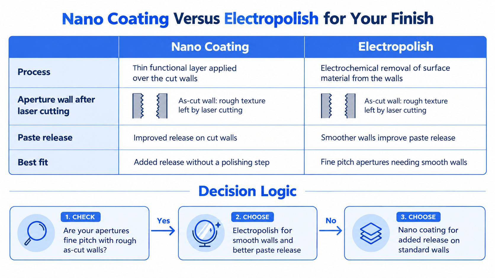
Electropolishing and nano coating aren't interchangeable claims. One addresses wall condition; the other adds a surface treatment. A supplier proposing either should explain the limitation it is intended to address.
The engineering discussion of solder paste and stencil design connects stencil geometry and paste volume with package stand-off and reliability. It also highlights an important qualification: improved initial release from a nano-coated stencil doesn't settle the question of long-term stability.
<a id="fix-geometry-before-buying-a-finish"></a>
Fix Geometry Before Buying a Finish
Start with suitable aperture proportions, rounded corners and justified reductions. For exposed thermal pads, evaluate segmented or windowpane openings as a way to regulate deposition and support flux outgassing, rather than treating the entire pad as one unrestricted opening.
Electropolish is a sensible candidate when inspected wall roughness appears to limit release. Nano coating deserves a trial when difficult apertures still need help after geometry and paste compatibility have been reviewed.
Neither upgrade should be automatic on a coarse-feature board. If an unfinished candidate meets the approved print and assembly requirements, an added finish needs a measurable benefit to justify its cost.
Qualification warning: A good first print proves initial performance. It doesn't prove coating life.
<a id="ask-for-production-evidence"></a>
Ask for Production Evidence
Request the finish process record, recommended cleaning method and inspection evidence representative of the supplied batch. Have the manufacturer quote the treatment separately so you can see what you're paying to evaluate.
Compare early and later print results under the intended cleaning routine. Track paste behavior and post-reflow outcomes, including voiding and component imbalance, rather than treating a smoother-looking deposit as the final result.
If the supplier recommends both treatments, ask what the combination adds beyond either treatment alone. The answer should be a testable proposition, not a premium finish label.
<a id="lead-times-moq-and-what-drives-stencil-pricing"></a>
Lead Times, MOQ and What Drives Stencil Pricing
SMT stencils at Lianyuhong start from $5.00 per piece. That entry point covers a laser-cut 304 HTA stainless steel foil in the 0.08–0.3 mm thickness range, before stepped regions, electropolish, nano coating or documentation are priced in. Compare suppliers at the same option stack, or the numbers mean nothing.
MOQ and lead time have no defensible published figures. Both depend on order type, finish load and current capacity, so they belong in the written quotation for your specific order.
| Order Type | What Moves the Quote | Yield Risk to Check | |---|---|---| | Prototype stencil, standard foil | Frame and foil specification | Foil thickness mismatched to the finest aperture family | | Stepped or multi-level stencil | Step count and region design | Local thickness changes that alter paste height on fine-pitch apertures | | Electropolished or nano-coated foil | The chosen treatment | A finish bought on its label rather than on measured release | | Production repeat order | Revision status and material stock | A reorder cut from an outdated drawing | | Revision after a Gerber change | Scope of change and recutting | An aperture edit that silently changes a qualified deposit |
<a id="pin-down-when-the-clock-starts"></a>
Pin Down When the Clock Starts
File receipt, engineering approval, payment release, fabrication completion and dispatch are five different milestones. A quoted lead time that starts at payment and ends at fabrication is a different promise than one ending at dispatch. Ask which milestone the schedule ends on, and what pauses it.
I've watched a fast cutting slot go to waste while an aperture-design question sat unanswered for days. The foil was never the bottleneck.
<a id="price-the-yield-risk-not-just-the-foil"></a>
Price the Yield Risk, Not Just the Foil
A foil at the entry price that fails your first print costs more than a stepped, finished foil that passes. On a mixed-pitch board, the pricing question is which upgrades the aperture families actually need for release, based on the pitch mix and the paste you qualified.
Compare quotes at the same deliverable level. A bare-foil price and a documented, finished-stencil price describe different products, and a documentation package means little unless its contents are named.
<a id="protect-the-assembly-schedule"></a>
Protect the Assembly Schedule
Send the complete engineering package with the quote request and state whether first-article approval gates production release. For a compressed build, coordinate stencil delivery with the wider quick-turn PCB assembly schedule, including materials and inspection readiness.
Keep revision timing separate from routine reorder timing. A familiar board name isn't evidence that the existing stencil still suits the current Gerber. Ask who approves the updated aperture drawing and whether the change requires a replacement foil.
<a id="qa-evidence-and-a-first-article-stencil-test"></a>
QA Evidence and a First-Article Stencil Test
| Control | What It Proves | Evidence to Request | |---|---|---| | Aperture dimensional check | Openings match the approved data within the agreed tolerance | Inspection report with identified sampled apertures | | Wall quality inspection | Wall condition meets the agreed fabrication requirement | Microscope photographs of cut and finished walls | | Foil thickness mapping | Thickness matches the approved local design | Readings tied to locations on the foil | | Finish verification | The specified treatment was applied | Batch process record | | Material traceability | Material identity connects to the delivered stencil | Certificate and lot record tied to its serial | | SPI on the first board | Actual deposited volume, height and area | Distributions by aperture family | | Transfer efficiency | Actual deposition relative to theoretical aperture volume | Calculations and acceptance results by family |
The supplier proves the foil; the assembly line proves the print. Dimensional conformity is necessary, but it doesn't demonstrate successful deposition with your paste and printer.
IPC research on stencil printing and transfer efficiency defines transfer efficiency as deposited paste volume divided by theoretical aperture volume, multiplied by 100. It describes conventional practice targeting roughly 70–80%, and reports nano-coating improvements of 10–24% as area ratio decreased from 0.67 toward 0.40.
Those are test-context results, not a supplier guarantee. The same guidance discusses a practical area-ratio limit of about 0.50 with ultrafine powders, subject to paste compatibility and defect-risk validation.
<a id="run-a-controlled-acceptance-trial"></a>
Run a Controlled Acceptance Trial
- Choose representative features. Include the smallest pitch, largest pad and aperture family most likely to print inconsistently. Don't qualify only convenient inspection locations.
- Print a verification coupon or first board using the intended production paste. Record the paste identity and condition.
- Measure with SPI. Collect volume, height and area across repeated prints. Preserve the results by aperture family rather than combining everything into a board-level average.
- Calculate transfer efficiency for difficult openings using their approved geometry and local foil thickness. Compare against the agreed trial criteria.
- Examine the tails. Review the mean, standard deviation and out-of-limit rate. A satisfactory average can conceal repeatedly underprinted or overprinted locations.
- Reflow the trial assembly. Use AOI and appropriate X-ray inspection for hidden joints, then connect the findings to the original deposits.
- Investigate in a defined order. Review registration and aperture geometry, then printing settings and cleaning behavior, before commissioning a different thickness or finish.
- Sign the report with the stencil serial, approved revision, paste lot, printer settings and acceptance limits.
When comparing stencil candidates, hold the paste, squeegee and printer setup constant. During troubleshooting, change one selected variable at a time and record the reason, otherwise you won't know which change helped.
<a id="close-the-loop-after-reflow"></a>
Close the Loop After Reflow
Include the stencil trial in the PCB prototype assembly acceptance plan, not as an isolated purchasing inspection. A print that looks acceptable still needs to produce acceptable joints.
If a problem appears after reflow, don't automatically blame the stencil. Use the recorded SPI results to establish whether deposition was out of control before changing the foil.
<a id="send-your-first-stencil-rfq-with-this-checklist"></a>
Send Your First Stencil RFQ With This Checklist
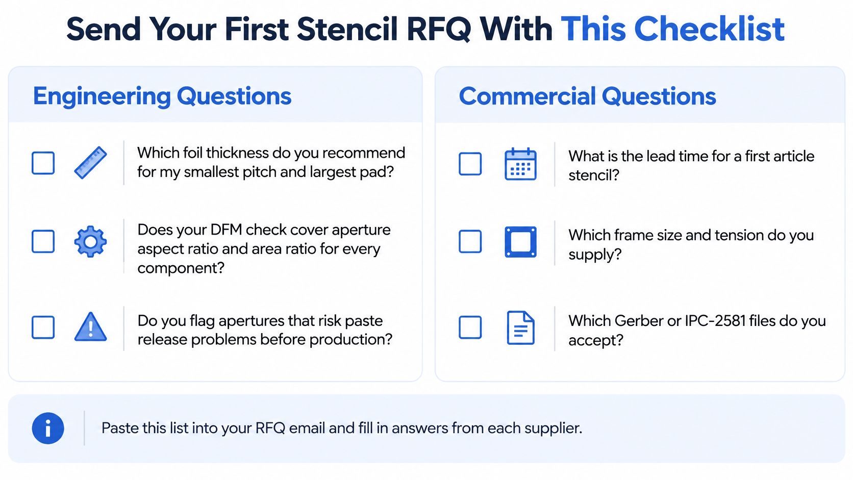
A useful RFQ makes competing suppliers answer the same engineering and commercial questions. You're not looking for the longest capability list. You're looking for a proposal you can approve, test and reorder without losing revision control.
<a id="engineering-questions"></a>
Engineering Questions
- Thickness selection. Which foil construction do you recommend for the smallest aperture and largest paste-volume requirement?
- DFM coverage. Does the review check both release ratios and flag difficult aperture families?
- Mixed-height support. Can you propose stepped or separate-print alternatives, and how will local thickness be verified?
- Dimensional acceptance. How do you measure aperture tolerance, and what sampling plan will appear in the report?
- Print validation. Who supplies SPI results by aperture family, and who signs the first-article release?
<a id="procurement-questions"></a>
Procurement Questions
- Traceability. Which material certificate and serial-linked records accompany the stencil?
- Finish evidence. What supports the release claim, and what cleaning or durability limitations apply?
- Delivery and price. What are the prototype, revision and reorder commitments, with frame, foil, finish, steps and rush charges separated?
- Revision control. How are approved Gerbers retained, and how do you prevent an obsolete foil from being reordered?
We offer laser-cut 304 HTA stainless-steel SMT stencils in 0.08–0.3 mm thicknesses, with nano-coating or electropolishing options, starting from $5.00 per piece. Don't assume that catalogue thickness range covers every fine-feature requirement; have engineering confirm suitability before ordering.
For a coordinated build, include stencil approval in your turnkey PCB assembly requirements. Send the Gerbers, pad-to-aperture drawing, board thickness and component list, state whether first-article review is required, and request a quotation with a sample test plan. Our secure upload process routes design files to engineers for DFM feedback before quotation.
Lianyuhong Technology Co.,Ltd offers SMT stencil manufacturing alongside PCB fabrication and assembly, allowing you to review the foil against the board's actual component mix. Visit Lianyuhong Technology Co.,Ltd to submit your files and request DFM feedback, a stencil quotation and an agreed first-article verification plan.