
You've placed the connectors, routed the signals, and folded the board into the enclosure model. Everything fits, until someone asks whether that flex section bends only during assembly or every time the product moves. That answer can change the required geometry before you've ordered a prototype.
Good rigid flex PCB design guidelines connect mechanical requirements to layout constraints, physical testing, and manufacturing documentation. Treat the flex region as a moving mechanical part that happens to carry signals, not as a thin rigid board.
Table of Contents
- Bend Radius Limits for Static and Dynamic Flex
- Building the Stack-Up Layer by Layer
- Protecting Transitions and Routing in the Bend Zone
- Choosing Copper, Coverlay and Stiffeners
- Validating and Diagnosing Bend Life
- What to Send Your Fabricator and Assembler
- Pre-Order Go or No-Go Check
<a id="bend-radius-limits-for-static-and-dynamic-flex"></a>
Bend Radius Limits for Static and Dynamic Flex
Minimum bend radius by bend type and flex construction
The following ratios and worked dimensions follow the IPC-2223E guidance summarized in the Cadence rigid-flex design checklist, with example radii calculated for 0.20 mm total flex thickness.
| Bend type | Flex construction | Minimum radius | Radius at 0.20 mm | |---|---|---|---| | Static, one-time fold | Single- or double-layer | 6× total thickness | 1.2 mm | | Static, one-time fold | Three or more flex layers | 12× total thickness | 2.4 mm | | Dynamic, repeated motion | Single-layer | 100× total thickness | 20 mm | | Dynamic, repeated motion | Double-layer | 150× total thickness | 30 mm | | Dynamic, repeated motion | Multilayer | 200× total thickness | 40 mm |
Read the table by choosing the bend category first, then the flex construction. A tail folded into an enclosure and held stationary has a different mechanical requirement from a service loop that moves with an actuator. The material stack might be identical, but the operating duty isn't.
Total thickness means the complete flexible construction: copper, dielectric, adhesive, and coverlay. Using only the polyimide core thickness understates the dimension that matters. Take the finished stack thickness from the proposed fabrication stack-up, not from a laminate name in the CAD library.
<a id="translate-the-radius-into-enclosure-geometry"></a>
Translate the radius into enclosure geometry
The example exposes a common packaging mistake. A single-layer tail that fits comfortably as an assembly fold may need much more room when used as a moving hinge. Adding flex layers makes that packaging problem harder, even when the electrical routing becomes easier.
Specify the radius at the innermost bend surface, rather than leaving the mechanical designer and PCB designer to choose different reference surfaces. Copper away from the neutral axis experiences greater strain as the bend tightens. Both the inner and outer sides matter because bending produces compression on one side and tension on the other.
Practical rule: A minimum-radius calculation is a geometry screen, not a guarantee of service life.
Don't turn a minimum-radius bend into a sharp crease. Leave allowance for stack thickness variation, assembly positioning, and the actual shape imposed by the enclosure. A folded CAD model should show the bend envelope, not merely the final positions of the rigid sections.
Before routing, create a bend record for every flex zone:
- Duty: Identify installation-only motion or repeated operation.
- Construction: Record the finished flex thickness and layer count.
- Geometry: Document the calculated radius, intended radius, and bend direction.
- Approval: Have electrical and mechanical owners sign off on the same envelope.
When defining the construction, distinguish a standalone flexible PCB from the flexible region of an integrated rigid-flex assembly. The local flexible stack, not the surrounding rigid-board thickness, controls the bend calculation.
<a id="building-the-stack-up-layer-by-layer"></a>
Building the Stack-Up Layer by Layer
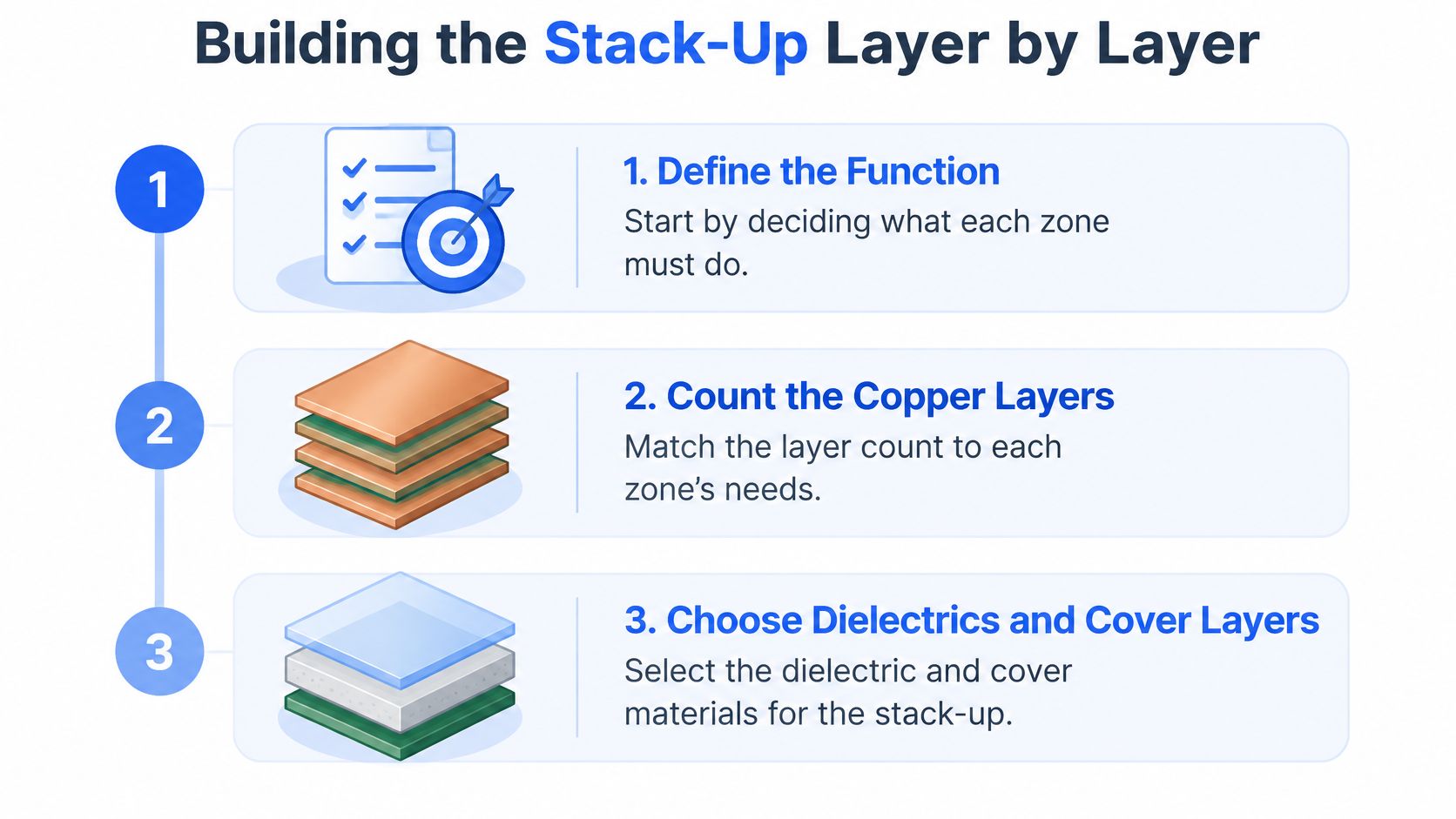
Start with what each region must do. A connecting tail, component-bearing island, and connector insertion area don't need the same construction. Assign functions before distributing signal layers across the board.
Use this sequence to organize the stack-up discussion.
Typical stack-up building blocks
| Construction | Copper layers | Core and cover | Typical use | |---|---|---|---| | Single-layer flex tail | Single conductor layer | Polyimide base with coverlay | One-time fold to connect boards | | Double-layer flex | Paired conductor layers | Polyimide core, coverlay on both faces | Fold or hinge with careful neutral-axis placement | | Multilayer flex section | Multiple conductor layers beyond a pair | Additional dielectrics and bonding layers increase height | Dynamic zones only when the larger radius fits and testing supports use | | Rigid section | Multilayer as electrically required | FR-4 core and prepreg | Component mounting, connectors, and power | | Stiffened zone | Same as the underlying circuit | Added stiffener under pads or connectors | Component support and connector insertion |
<a id="read-the-construction-from-surface-to-surface"></a>
Read the construction from surface to surface
For a simple flex tail, start at the protective coverlay, identify its adhesive, then the copper and polyimide base. For a double-sided construction, continue through the core to the opposite copper and protective layers. Don't omit bonding films because they aren't electrical layers.
A multilayer flex adds routing capacity, but it also adds material that must bend. Don't extend every rigid-section layer through the flexible span just because the CAD tool allows it. Reserve flex layers for signals and references that need to cross that span.
The neutral axis is the region through the thickness that changes length least during bending. Copper closer to it sees less strain than copper farther away. Layer placement therefore matters alongside layer count, although the actual neutral-axis position depends on the materials and their stiffness, not just the geometric midpoint.
<a id="balance-electrical-and-mechanical-requirements"></a>
Balance electrical and mechanical requirements
Keep copper distribution reasonably balanced across rigid sections to reduce distortion during lamination and assembly. In the flexible section, review plane coverage and adjacent-layer conductor placement rather than treating copper balance as a reason to add unnecessary metal.
Adhesive-based and adhesiveless constructions also produce different finished thicknesses. Record the construction selected, including any separate coverlay adhesive that remains.
Develop PCB impedance control alongside this stack-up, not after routing. A trace geometry selected for the rigid region may need different dimensions or reference treatment in the flex.
Finish with a surface-to-surface record of material, thickness, copper weight, and regional extent. The fabricator must be able to build the intended structure without guessing which layers continue through each zone.
<a id="protecting-transitions-and-routing-in-the-bend-zone"></a>
Protecting Transitions and Routing in the Bend Zone
Keep vias, plated holes, component pads, and abrupt stiffener edges outside the active bend region. These features interrupt an otherwise compliant structure and concentrate load. Treat the rigid-to-flex transition as a strain-management feature, not just a line where the board changes color.
The flexible bridge needs room to curve without forcing the bend against either rigid edge.
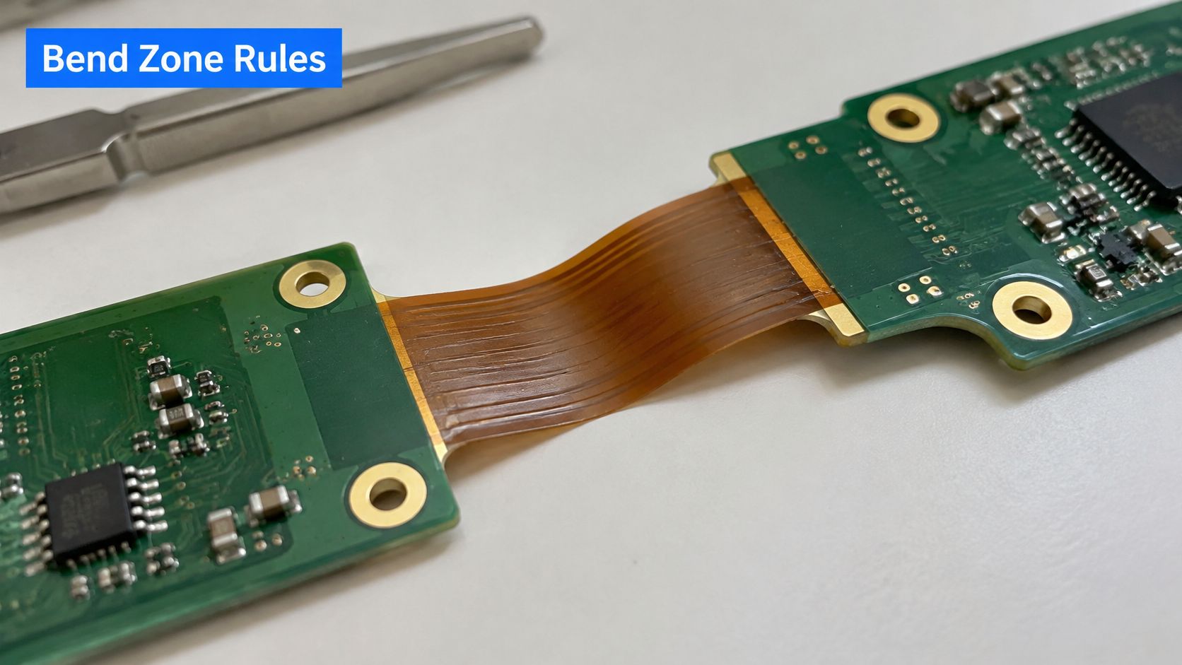
The Sierra Circuits IPC-2223 design-violation guide identifies at least 20 mils between vias and the interface as a reference clearance, while acknowledging that construction and fabrication capability can require larger distances. Don't treat that reference as universal approval for placing a via immediately outside the nominal boundary.
<a id="apply-routing-and-shaping-rules-together"></a>
Apply routing and shaping rules together
- Define the bend line: Draw the bend axis and motion direction explicitly. Route crossing conductors across that line, rather than along it.
- Remove abrupt geometry: Use rounded trace corners, teardrops, and filleted pad entries outside the moving span.
- Stagger conductors: Avoid directly superimposing adjacent-layer traces where practical, which can create a locally stiff strip.
- Coordinate support edges: Dimension coverlay overlap and stiffener termination so assembly doesn't force bending at an unsupported edge.
Published routing language can be confusing because authors use “bend direction” to mean different things. An axis is the line around which the circuit bends; the curved path runs across that axis. Include both on the drawing instead of approving a note that only says “parallel” or “perpendicular.”
Use the video alongside the board model when reviewing how the flexible region connects the rigid sections.
<iframe width="100%" style="aspect-ratio: 16 / 9;" src="https://www.youtube.com/embed/tfZvBdLZOLs" frameborder="0" allow="autoplay; encrypted-media" allowfullscreen></iframe><a id="make-the-rules-enforceable"></a>
Make the rules enforceable
Enter feature-specific keep-outs into the CAD constraint system. Block vias and components without accidentally prohibiting the signal traces that must cross the flex. Then inspect the folded model for interference, edge contact, and unintended bend migration.
Near fine-pitch BGA escape routing, don't assume a clean automated optical inspection result proves mechanical integrity. A damaged conductor or plated feature can require continuity cycling or cross-section analysis to diagnose. Release the layout only after the transition geometry and fabrication clearances agree.
<a id="choosing-copper-coverlay-and-stiffeners"></a>
Choosing Copper, Coverlay and Stiffeners
Polyimide is the usual starting point for flexible regions because it accommodates bending and assembly heat. Its presence alone doesn't make a stack suitable for continuous motion. Copper condition, protective layers, bonding materials, and local reinforcement all affect the result.
Coverlay is typically a polyimide film bonded over the flex copper with adhesive. Use a cover system qualified for the intended motion rather than carrying ordinary rigid-board solder mask into an active bending region.
Copper and base material choices by bend category
| Material | Best bend category | Evidence and note | |---|---|---| | Polyimide base | Flexible zones, static and dynamic | Accommodates bending and soldering heat; qualify the finished construction | | Rolled annealed copper | Dynamic bend zones | Preferred candidate for repeated motion; confirm fatigue performance with production-representative testing | | Electrodeposited copper | Static one-time bends | Commonly used where repeated flexing isn't required; don't assume dynamic suitability |
A 2025 PCBMASTER design guide reports 50% better fatigue resistance for rolled copper foil in dynamic-bending areas, but doesn't identify an independent primary study for that comparison. Treat the figure as directional evidence for material selection, not as a service-life multiplier for your product.
<a id="select-support-without-creating-a-new-hinge"></a>
Select support without creating a new hinge
FR-4 stiffeners can support connectors and component-bearing areas. Polyimide stiffeners can provide local thickness or reinforcement where a bulky rigid backing isn't appropriate. In either case, keep the support termination away from the intended moving span and consider a gradual transition where the construction permits it.
A stiffener should support the connection, not move the fatigue problem to its own edge.
Adhesive-based constructions may be easier to source, but their bonding layers add thickness. Adhesiveless laminates can reduce that contribution; they don't necessarily eliminate adhesive elsewhere in the finished assembly. Compare complete proposed builds rather than material labels.
Create a material schedule by zone. State the copper type, base laminate, coverlay, bonding system, and stiffener material, then associate each zone with its intended bend duty. If sourcing proposes a substitute, review its mechanical implications before approving it as an electrical equivalent.
<a id="validating-and-diagnosing-bend-life"></a>
Validating and Diagnosing Bend Life
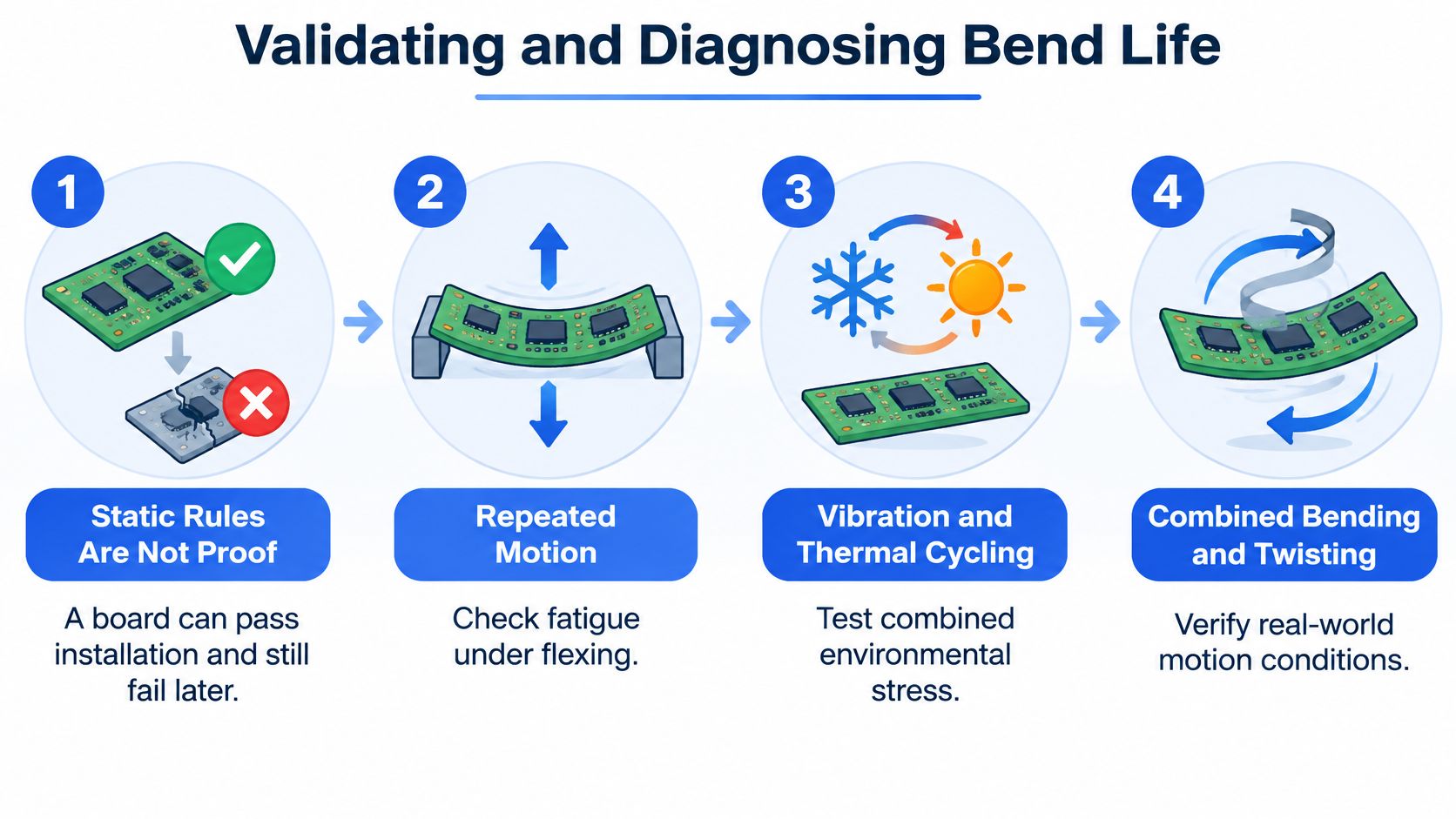
A board that survives installation hasn't demonstrated operating life. Repeated movement, vibration, temperature changes, and torsion can load it differently from a careful manual fold. The JLCPCB rigid-flex circuit guide provides broader construction guidance, but application-specific acceptance still requires a documented mechanical test plan.
These are separate questions: does the geometry satisfy the design rules, and does the manufactured construction survive the intended use? Record answers to both.
<a id="turn-the-motion-requirement-into-a-test"></a>
Turn the motion requirement into a test
The Altium rigid-flex design guidelines.pdf) emphasize reproducing the actual bend angle, radius, temperature, and cycle count while monitoring continuity. Use those conditions to define the fixture and instrumentation before the prototype arrives.
-
Record the complete load case. Specify bend radius, angle, cycle count, speed, temperature, torsion, and fixture constraints. Include installation handling and service access, since normal operation may not produce the tightest bend.
-
Identify the neutral axis and moving span. Mark the active bend region on the mechanical drawing and explain which surfaces the fixture constrains. This prevents the test technician from creating a different bend by clamping the sample differently.
-
Audit the released CAD data. Confirm that prohibited vias, pads, and components aren't inside the active zone. Check the exported manufacturing files as well as the editable design so a stale drawing doesn't reach the test supplier.
-
Build representative coupons. Match production copper, dielectric, coverlay, bonding, and relevant transition geometry. A bare laminate strip won't represent a finished circuit containing patterned copper and support edges.
-
Cycle under monitored continuity. Reproduce the specified radius and angle, and log electrical behavior during motion rather than only checking afterward. Set the acquisition method to capture brief interruptions that a stationary end-of-test check could miss.
-
Apply the environmental profile. Add vibration and thermal cycling appropriate to the field conditions. Where bending and twisting occur together, reproduce their combination rather than assuming separate tests are equivalent.
-
Investigate failures physically. Preserve the failed sample and record its bend position before sectioning. Compare crack location with the proposed mechanism; don't assume every open circuit means the bend radius was too small.
-
Set acceptance before testing. Define the required endurance, allowable resistance behavior, interruption criteria, and visual damage limits. Log failures and corrective actions against the exact drawing and material revision.
<a id="diagnose-by-symptom-then-confirm"></a>
Diagnose by symptom, then confirm
Rigid-flex failure symptoms, causes and prevention
| Symptom | Likely cause | Prevention | |---|---|---| | Intermittent opens after installation | Bend tighter than the static ratio | Recalculate radius from full stack thickness with margin | | Cracked barrel or lifted pad at transition | Via or pad inside the keep-out | Relocate the feature and use teardrops or filleted pad entries | | Coverlay tearing at an inner corner | Sharp internal corner | Use generous internal radii and appropriately staggered openings | | Failure after many hinge cycles | Static rule used on a dynamic zone | Select dynamic geometry and cycle-test representative coupons | | Impedance drift between rigid and flex | Undefined stack or changed adhesive | Specify the full stack and measure both sections | | Vibration failure near stiffener edge | Abrupt support termination inside the moving span | Adjust the stiffener termination and provide strain relief |
These are diagnostic starting points, not automatic verdicts. Check fixture damage, manufacturing variation, and handling history before changing the layout. A cross-section can distinguish a conductor crack from a plated-barrel problem that requires a different correction.
Use the applicable PCB design standards to organize construction and acceptance requirements, then add the product-specific motion test. Standards compliance and successful optical inspection don't replace evidence that the actual assembly survives its intended duty.
<a id="what-to-send-your-fabricator-and-assembler"></a>
What to Send Your Fabricator and Assembler
Layout, fabrication, and assembly teams need a shared definition of the board. If a stack drawing omits adhesive or leaves a stiffener location open to interpretation, CAM staff must make assumptions that the mechanical designer may never see.
The AIVON rigid-flex DFM case discussion connects incomplete stack and transition definitions with manufacturing and inspection risks. It also cautions that ±5% or ±8% impedance targets aren't automatically achievable without controlled construction and suitable test structures.
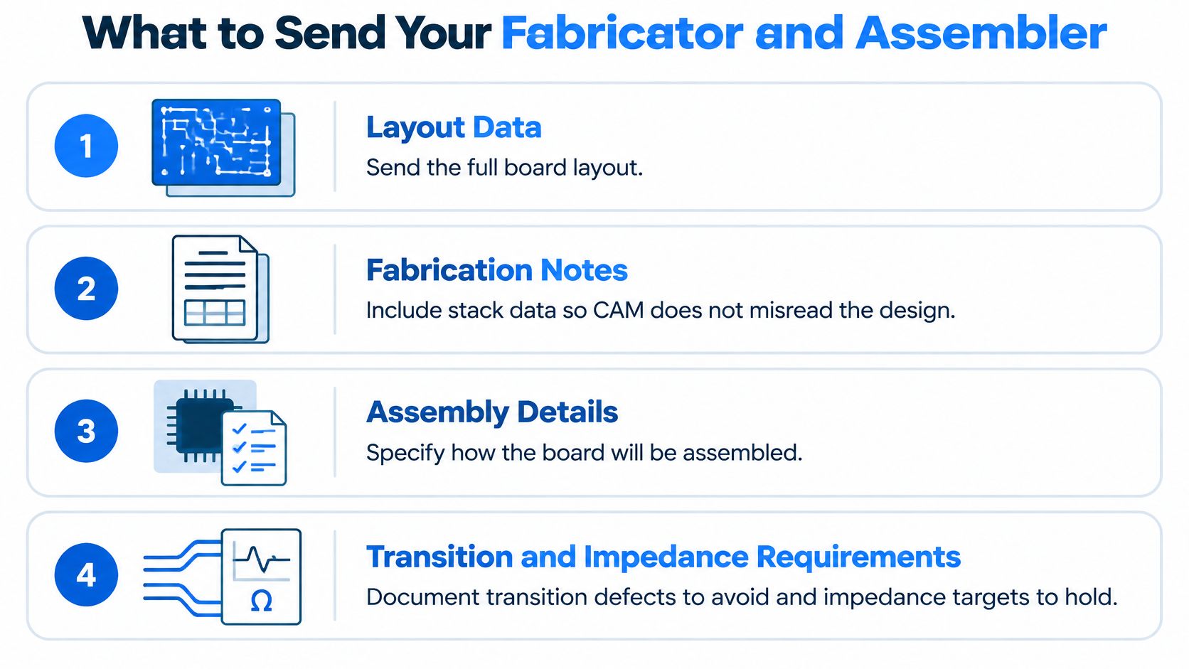
Organize the release so each team receives the same revision and acceptance basis.
<a id="attach-the-package-to-every-revision"></a>
Attach the package to every revision
- Layer-by-layer stack-up: Include thicknesses, materials, regional layer extents, and approved substitution controls. This prevents CAM from reconstructing an ambiguous stack.
- Mechanical and transition drawings: Dimension boundaries, keep-outs, internal corner radii, bend envelopes, and stiffener locations. These control tearing risks and exposure paths near transition vias.
- Electrical verification structures: Include rigid, flex, and transition coupons where required. Measuring only a rigid coupon doesn't characterize the complete interconnect.
- Assembly instructions: Supply the BOM, pick-and-place data, support requirements, and folding sequence. Identify where handling tools and fixtures may contact the board.
- Acceptance requirements: State the applicable IPC class, inspection limits, electrical tests, and mechanical qualification criteria. Define where AOI, X-ray, and destructive analysis apply rather than listing inspection methods without a purpose.
- Revision ownership: Assign someone to approve DFM changes and ensure the assembler receives the accepted manufacturing revision.
<a id="resolve-trade-offs-before-release"></a>
Resolve trade-offs before release
Hatched copper and fewer flex layers can improve compliance, but they may change shielding and impedance. Conversely, adding copper to preserve an electrical reference can make the moving section less compliant. Require electrical and mechanical approval for either change.
Keep qualification evidence linked to the construction that produced it. A material substitution, revised support edge, or changed bonding layer may require renewed analysis or testing, even when the schematic hasn't changed.
<a id="pre-order-go-or-no-go-check"></a>
Pre-Order Go or No-Go Check
An unresolved mechanical requirement is a no-go, not a purchasing note. Before authorizing the order, make the release owner confirm that the design and its evidence agree.
- Motion is defined: Every flex zone has an assigned duty and approved bend envelope.
- Construction is fixed: The layer record and material schedule match the released layout.
- Constraints are visible: Bend direction, exclusion zones, and support geometry appear on controlled drawings.
- Validation is actionable: The test plan contains measurable pass and fail criteria.
- Manufacturing changes are controlled: DFM responses identify who approves deviations and which files change.
Order against an approved revision, not against an email description of what the board should become.
Our secure-portal process starts with Gerber, BOM, and pick-and-place uploads. Engineers review the design and component availability for DFM feedback, followed by a detailed quotation with pricing and lead-time options, then manufacture, assembly, testing, and shipping.
Include the mechanical release package with those files. In the review request, require confirmation that our proposed rigid-flex production route supports your layer count, minimum trace width, and via construction. Close every discrepancy against the same drawings your design team approved before placing the order.
Lianyuhong Technology Co.,Ltd offers rigid-flex fabrication, PCB layout and DFM review, and turnkey assembly to connect design decisions with production requirements. Visit Lianyuhong Technology Co.,Ltd and submit your Gerber, BOM, pick-and-place files, stack-up, and bend-validation requirements so the engineering review addresses the board you intend to build.