
The most common advice about an impedance control PCB is to calculate the trace width and tell the fabricator to hold it. That's incomplete. Impedance control is a specification and acceptance problem before it's a routing problem: unless the drawing defines what gets built, what gets measured, and how the result is judged, the designer and manufacturer can both follow their instructions and still disagree about whether the board passes.
Table of Contents
- Why Impedance Control Matters More Than the Trace Width
- How Transmission Lines Actually Behave on a PCB
- Microstrip and Stripline Topologies Compared
- Stack-Up and Material Selection That Actually Sets the Number
- The Formulas and a Worked 50 Ohm Example
- Simulation and Verification Before the Fab Ever Sees the File
- Measurement Methods That Actually Catch a Bad Stack-Up
- DFM, BOM, and the Handoff Checklist to Your Manufacturer
<a id="why-impedance-control-matters-more-than-the-trace-width"></a>
Why Impedance Control Matters More Than the Trace Width
A trace width is a manufacturing dimension. A characteristic impedance is an electrical property of the finished transmission-line structure. Treating them as interchangeable leaves too much room for interpretation between layout release and incoming inspection.
The practical question isn't whether the fabricator can reproduce a line in the artwork. It's whether the fabricator can reproduce the intended electrical structure, demonstrate that it meets an agreed requirement, and provide evidence tied to the delivered production lot.
<a id="separate-the-design-target-from-the-acceptance-requirement"></a>
Separate the design target from the acceptance requirement
The design target belongs in the electrical definition of the interface. The acceptance requirement belongs in the fabrication drawing and purchase order. They should agree, but they serve different purposes.
A useful release package separates these responsibilities:
- Electrical intent: Identify the controlled nets, their signaling mode, their routing layers, and their intended references.
- Manufacturing definition: Identify the approved stack-up, material construction, and geometry that the fabricator will build.
- Acceptance evidence: Define the test structure, measurement procedure, evaluation window, and production sampling.
- Change authority: State which adjustments the fabricator may make and which require engineering approval.
A note that specifies only a nominal impedance leaves the last two responsibilities unresolved. One laboratory might evaluate a relatively uniform region of the trace; another might include the launch transition. Without an agreed evaluation rule, the disagreement is partly contractual, not necessarily a manufacturing failure.
Practical rule: If the purchase order doesn't explain how a board can fail, it doesn't fully explain what passing means.
<a id="decide-who-owns-the-final-geometry"></a>
Decide who owns the final geometry
The layout engineer shouldn't freeze dimensions that the fabricator cannot hold. Equally, the fabricator shouldn't alter critical routing to achieve an electrical target.
Require a proposed production stack-up before release. Have the SI engineer review changes to controlled geometry, and have procurement attach the approved revision to the order. The contract manufacturer should receive that same revision rather than reconstructing requirements from an old quotation.
That discipline turns impedance control from a selectable ordering option into an auditable requirement. It also makes a later failure investigation much more useful: the team can compare an agreed construction and test procedure instead of debating what an isolated number was supposed to mean.
<a id="how-transmission-lines-actually-behave-on-a-pcb"></a>
How Transmission Lines Actually Behave on a PCB
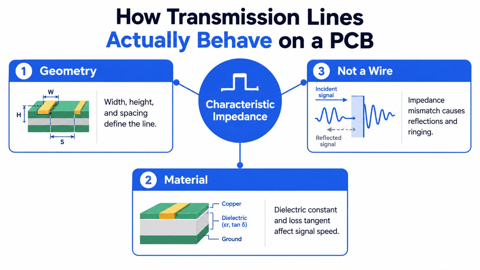
A PCB trace isn't electrically independent of its surroundings. Its transmission-line behavior depends on the conductor, the dielectric around it, and the return path that completes the electromagnetic structure.
Characteristic impedance describes the relationship between voltage and current for a traveling wave along that structure. It isn't the resistance a handheld meter measures between the ends of the copper. A trace can have low DC resistance and still present an unsuitable transmission-line impedance.
The relationships are easier to understand when geometry, material, and discontinuities are considered together.
<a id="follow-the-edge-not-just-the-clock"></a>
Follow the edge, not just the clock
Whether a connection needs transmission-line treatment depends on how quickly the signal changes relative to its propagation along the route. A slowly repeating signal can still have a fast edge. Evaluating only its repetition frequency can therefore miss the behavior that matters.
A water-pipe analogy helps with the intuition. A pressure disturbance traveling through a pipe encounters a change when the pipe geometry changes; some disturbance continues, and some returns. On a PCB, the relevant boundary is an electrical impedance change rather than merely a visible change in width.
That reflected energy can combine with subsequent portions of the waveform. Depending on the channel and termination, the receiver may see ringing, overshoot, or an unsettled transition. Termination is part of the transmission-line design, not a substitute for defining the line itself.
<a id="distinguish-impedance-from-loss"></a>
Distinguish impedance from loss
Material selection introduces another distinction:
- Dielectric constant, Dk: Use it when evaluating field distribution, propagation, and impedance for a particular construction.
- Dissipation factor, Df: Evaluate it as part of dielectric loss, rather than treating it as another name for impedance.
- Return-path continuity: Inspect the reference structure along the route, including changes near vias and connectors.
A nominally correct impedance doesn't establish that a long channel has acceptable loss. Likewise, choosing a lower-loss material doesn't repair a broken return path.
When reviewing a cross section, ask where the fields extend and which conductors provide the return reference. Then inspect whether that structure continues along the actual route. Eye closure, timing uncertainty, emissions, and reduced link margin are system-level concerns; they can't be assessed from a trace-width entry alone.
<a id="microstrip-and-stripline-topologies-compared"></a>
Microstrip and Stripline Topologies Compared
Choose the reference-plane arrangement before choosing a routing width. Otherwise, the layout team may optimize a geometry that becomes invalid as soon as the stack-up changes.
Surface microstrip, embedded microstrip, symmetric stripline, and asymmetric stripline represent different field environments. None is automatically the right choice for every controlled net.
<a id="microstrip-vs-stripline-topologies"></a>
Microstrip vs Stripline Topologies
| Topology | Reference Planes | Typical Use | Key Trade-off | |---|---|---|---| | Surface microstrip | An underlying reference plane | Outer-layer routing and connections to surface components | Accessible routing, but the surrounding surface environment remains part of the construction | | Embedded microstrip | An underlying reference plane, with dielectric covering the trace | Buried routing with a microstrip-style reference arrangement | Requires the overlying dielectric to be included in the model | | Symmetric stripline | Reference planes with the trace centered between them | Internal routing where a balanced reference geometry fits the stack-up | Requires a suitable centered construction and internal access transitions | | Asymmetric stripline | Reference planes at unequal distances from the trace | Internal routing constrained by practical multilayer construction | The model must retain the unequal reference distances |
For surface microstrip, the field environment includes the board surface. Solder mask and nearby copper therefore belong in the geometry review where relevant. Don't use a bare-conductor calculator result as though it describes every finished outer-layer construction.
Embedded microstrip needs similar care with terminology. A buried trace isn't automatically symmetric stripline. The surrounding conductors and dielectric arrangement determine the topology, not the fact that the trace is hidden.
<a id="select-the-topology-by-routing-constraints"></a>
Select the topology by routing constraints
Symmetric stripline is useful when the stack-up can accommodate a centered signal layer between suitable reference planes. But the full route still needs transitions to components or connectors. Evaluate those transitions rather than assuming an internal route makes the whole channel uniform.
Asymmetric stripline accommodates unequal distances to the surrounding planes. That can fit a practical stack-up well, provided the fabricator and designer use the same cross section in their calculations.
Choose the topology that preserves the intended reference along the route, not the topology with the most appealing calculator result.
Interface names alone aren't sufficient selection rules. USB, HDMI, PCIe, and DDR routing must follow their actual component placement, breakout constraints, reference plan, and channel requirements. A connector-facing route and a buried interconnect can justify different constructions even within the same product.
The useful comparison is therefore buildability versus routing needs. Ask whether the chosen topology can be manufactured consistently, accessed sensibly, and represented faithfully by the production coupon.
<a id="stack-up-and-material-selection-that-actually-sets-the-number"></a>
Stack-Up and Material Selection That Actually Sets the Number
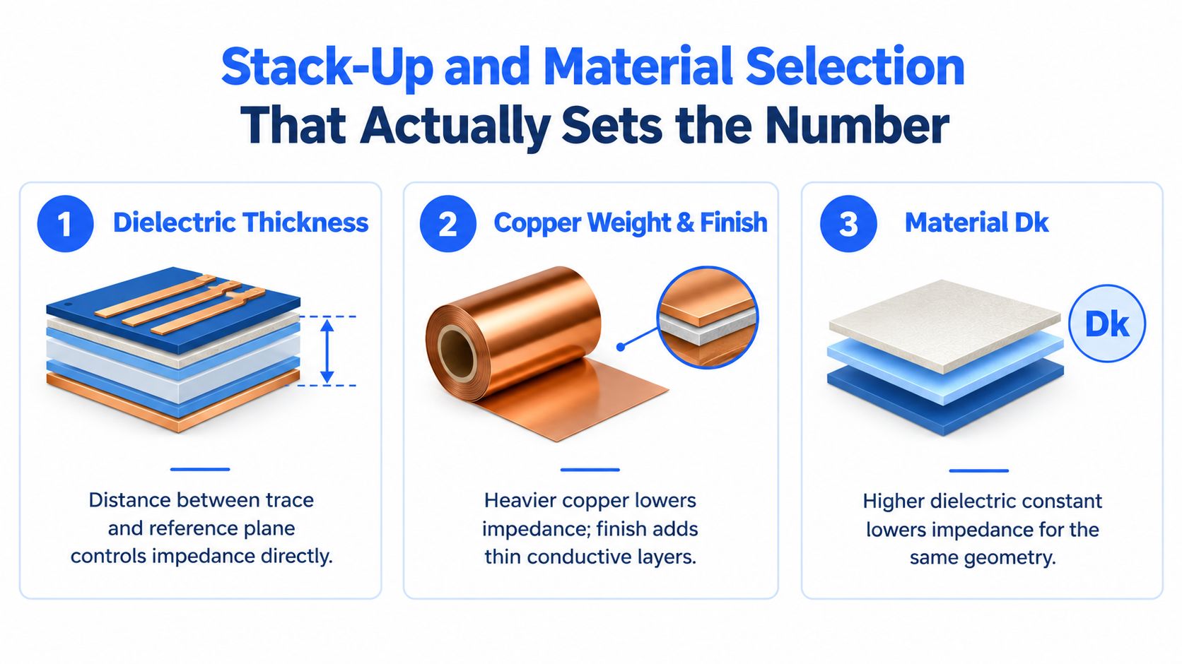
Start the stack-up discussion with the fabricator's proposed construction, not a generic material label. The electrical model needs the dielectric spacing and finished conductor geometry that production will deliver.
The main relationships are shown below. Treat them as directional guidance, not permission to change an input without recalculating the complete structure.
<a id="review-finished-construction-rather-than-catalog-labels"></a>
Review finished construction rather than catalog labels
Dielectric separation is the distance between the signal conductor and its reference structure. Overall board thickness doesn't identify that distance. Ask the fabricator to distinguish the relevant finished dielectric dimensions from the total mechanical thickness.
Copper geometry needs equally careful treatment. Starting foil, plating where applicable, and etching contribute to the final cross section. A nominal artwork width doesn't fully describe the finished conductor, particularly when the etched profile isn't rectangular.
Material comparisons should begin with the application's electrical, thermal, and manufacturing requirements:
- FR-4 and high-Tg FR-4: Evaluate the specific construction and electrical properties. A thermal designation alone isn't an electrical loss specification.
- Rogers RO4000-series and PTFE-based laminates: Consider these candidates when the RF or channel-loss requirements justify a different material system, then confirm fabrication constraints.
- Alumina and aluminum-nitride ceramics: Review electrical construction alongside thermal and assembly requirements rather than treating ceramic as a direct laminate replacement.
- Metal-core substrates: Start with the thermal architecture, then establish whether the required signal-reference structure is practical.
For an RF construction review, the relevant high-frequency PCB fabrication options provide a starting point for discussing material availability and stack-up feasibility. The material family name should lead to a specific construction proposal, not end the discussion.
<a id="spend-tolerance-where-the-interface-needs-it"></a>
Spend tolerance where the interface needs it
The IPC-oriented controlled-impedance guidance describes ±10% as common for slower digital interfaces and ±5% around 10–25 Gbps, with tighter control considered for demanding links such as 25G/50G/100G SerDes and RF applications. Those are industry-practice guidelines, not substitutes for the interface's own electrical requirements.
A tighter tolerance can constrain material substitutions and geometry adjustments. Don't buy it because the number looks more rigorous. First establish whether the channel needs that manufacturing window and whether the proposed process can demonstrate compliance.
Use the following video as supplementary context while reviewing the proposed construction with engineering.
<iframe width="100%" style="aspect-ratio: 16 / 9;" src="https://www.youtube.com/embed/s2BomzmM5W8" frameborder="0" allow="autoplay; encrypted-media" allowfullscreen></iframe><a id="the-formulas-and-a-worked-50-ohm-example"></a>
The Formulas and a Worked 50 Ohm Example
A useful calculation must begin with a defined cross section. Without one, a worked result is only an illustration of assumptions, not a recommendation for production trace width.
For a uniform transmission line, the low-loss relationship can be expressed symbolically as:
Z₀ ≈ √(L′ / C′)
Here, L′ and C′ represent inductance and capacitance per unit length. This relationship explains why impedance belongs to the complete structure: changing the conductor or reference environment changes those distributed properties.
<a id="use-topology-specific-approximations-carefully"></a>
Use topology-specific approximations carefully
IPC-2141A is a controlled-impedance design guide addressing formulas and coupons. Microstrip and stripline approximations must be used within the geometry they describe; they aren't interchangeable recipes.
For microstrip, the calculation needs trace width, conductor thickness, reference separation, and the relevant dielectric description. Stripline requires the surrounding plane arrangement as well. Differential calculations need the relationship between the paired conductors.
A hand calculation is useful for detecting an implausible proposal. It isn't sufficient evidence that a particular production process will hold the requested acceptance band.
<a id="work-the-target-backward-into-a-buildable-geometry"></a>
Work the target backward into a buildable geometry
For the nominal target in this example, use the fabricator's proposed cross section rather than inventing a board construction:
- Establish the baseline: Enter the proposed material properties, finished dielectric separation, and finished copper geometry.
- Solve the width: Adjust the conductor width until the model reaches the required nominal impedance.
- Perturb the dielectric: Evaluate the fabricator's stated finished-thickness limits.
- Perturb the conductor: Evaluate the permitted finished-width range and etched profile.
- Review material assumptions: Recalculate with the agreed electrical-property limits, keeping other inputs unchanged.
The result should be a sensitivity worksheet, not just a preferred width. Record which input changed, what remained fixed, and whether the resulting impedance stayed inside the required manufacturing window.
Calculation discipline: Don't substitute assumed dimensions for missing fabrication data and then treat the output as a verified design.
If the proposed width is difficult to manufacture or route, revisit the construction. Don't force the layout around a calculator result before discussing alternatives with the fabricator.
The engineering deliverable is an agreed geometry and its assumptions. A field-solved result based on that geometry can support release; an unexplained nominal output cannot.
<a id="simulation-and-verification-before-the-fab-ever-sees-the-file"></a>
Simulation and Verification Before the Fab Ever Sees the File
Simulation should answer progressively broader questions. First, can the proposed cross section meet the target? Next, does the routed board preserve that structure? Finally, does the complete channel meet the receiver's requirements?
Those questions require different models. Using a detailed channel model before confirming the fabrication inputs creates precision without a dependable foundation.
<a id="separate-cross-section-work-from-channel-work"></a>
Separate cross-section work from channel work
Use a cross-sectional field solver for uniform single-ended and differential routing. Confirm the topology, dielectric construction, copper profile, mask where applicable, and nearby reference conductors. Save those inputs with the stack-up revision.
Use a spatial model for regions that don't resemble a uniform cross section, such as vias, connector transitions, and complex component breakouts. The point isn't to model every millimeter with maximum detail. It's to apply suitable detail where the structure changes.
Post-layout review should include:
- Rule compliance: Check that controlled nets use the approved layer-specific widths and spacing.
- Exceptions: Identify neck-downs, coupled regions, and route segments that depart from the nominal geometry.
- Transitions: Review layer changes and component connections as channel structures.
- Operating margin: Evaluate the channel with the relevant driver, receiver, package, and termination assumptions.
SI and PI review should remain coordinated without conflating their acceptance criteria. An impedance coupon won't establish power-delivery performance, and a satisfactory power-distribution simulation won't validate a signal transition.
The engineering review should inspect the underlying models, not only the final eye diagram.

<a id="freeze-the-assumptions-with-the-layout"></a>
Freeze the assumptions with the layout
A PCB layout and engineering review should deliver traceable inputs alongside the routing files. Include the approved stack-up, controlled-net classes, model assumptions, and disposition of exceptions.
Hand formulas are a starting point, not an acceptance tool. Simulation supports the design decision; production measurement checks the manufactured result. Neither eliminates the need for the other.
Before release, make sure the modeled structure and the proposed test structure describe the same intended construction. If they differ, resolve that difference before procurement places the order.
<a id="measurement-methods-that-actually-catch-a-bad-stack-up"></a>
Measurement Methods That Actually Catch a Bad Stack-Up
A report marked “impedance passed” isn't enough. Ask what structure was measured, how the instrument was calibrated, and which part of the response determined the verdict.
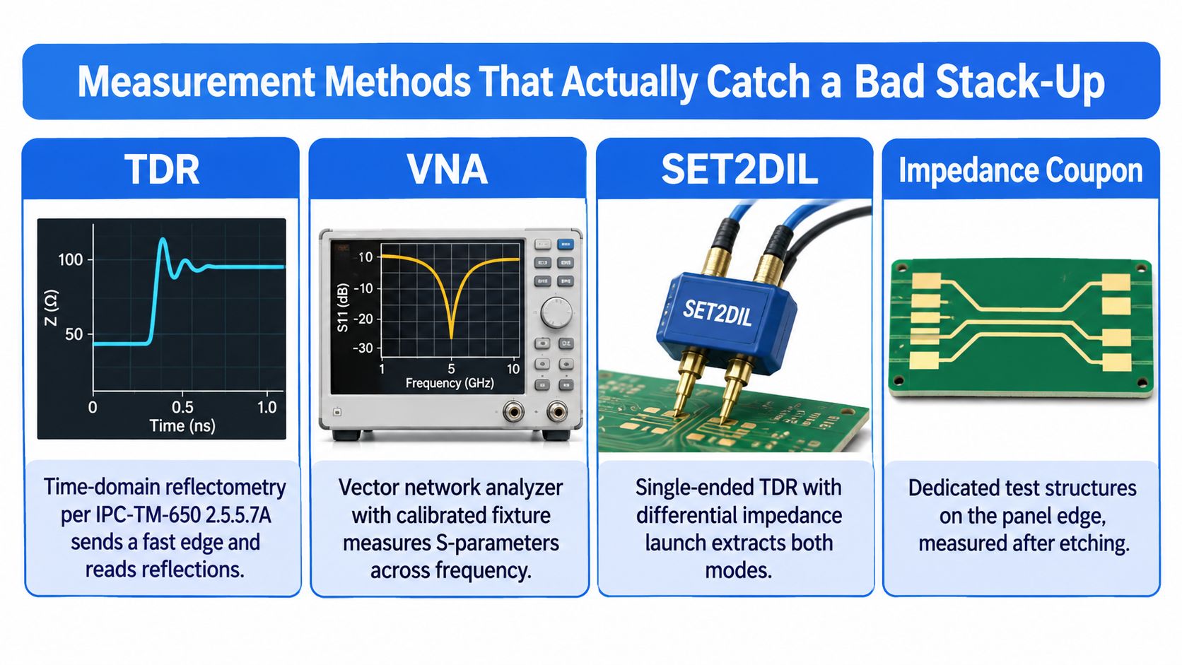
IPC-TM-650 2.5.5.7A is the relevant TDR measurement method identified in the controlled-impedance guidance discussed earlier. Naming it establishes a measurement reference, but the purchase order still needs the product-specific coupon and acceptance details.
The methods below address related but different questions.
<a id="match-the-method-to-the-evidence-required"></a>
Match the method to the evidence required
| Method | Evidence to request | Acceptance limitation | |---|---|---| | TDR | Impedance waveform, calibration details, launch arrangement, and evaluation window | A reported average can conceal features outside the evaluated region | | VNA | Calibrated S-parameter data, fixture definition, and any de-embedding procedure | Fixture effects must be distinguished from the structure under test | | SET2DIL | Exact procedure, coupon drawing, equipment configuration, and reported quantity | The method name alone doesn't define the delivered acceptance evidence | | Delta-L | Defined coupon structures, extraction procedure, and reported loss result | A loss result doesn't independently establish compliance with an impedance requirement |
TDR is useful when the acceptance question concerns impedance along a test structure. The evaluation window matters: a launch transition, a uniform routing region, and an end reflection aren't interchangeable portions of the waveform.
VNA measurements support frequency-domain channel evaluation. Require an explicit account of the fixture and calibration reference planes rather than assuming the instrument measures only the intended PCB structure.
SET2DIL and Delta-L should not be accepted as unexplained alternatives merely because they appear on a capability list. In particular, loss characterization and impedance acceptance are different deliverables. Agree on the procedure and the quantity that determines pass or fail.
<a id="make-the-coupon-representative"></a>
Make the coupon representative
The coupon must reproduce the product's relevant stack-up, reference-plane configuration, trace geometry, and differential spacing. Otherwise, a passing coupon can coexist with product routing that behaves differently.
A coupon validates the construction it represents. It doesn't certify every transition or exception on the product.
Specify the coupon's layer assignment, reference arrangement, conductor construction, and relationship to the controlled routing. Then define the averaging or gating rules, treatment of local excursions, and lot-level sampling plan.
Require records that connect the measurement to the delivered lot and approved drawing revision. When results are disputed, retained waveforms and coupon identification are more useful than a pass label without context.
<a id="dfm-bom-and-the-handoff-checklist-to-your-manufacturer"></a>
DFM, BOM, and the Handoff Checklist to Your Manufacturer
Put the acceptance language in the fabrication drawing and purchase order, not only in email. Use the following template, replacing the bracketed fields before release.
Controlled-impedance requirement
Controlled nets and layers: [net classes and routing layers].
Target and mode: [nominal impedance; single-ended or differential].
Tolerance: [approved acceptance band].
Design reference: IPC-2141A.
Test reference: IPC-TM-650 2.5.5.7A, with [agreed setup and calibration].
Construction: [approved stack-up revision and coupon drawing].
Evaluation: [waveform window, averaging or gating, and excursion rules].
Sampling: [lot definition, sample selection, retest, and disposition rules].
Records: [required results, traceability, and retention].
Changes: [approval required for material or geometry substitutions].
<a id="release-the-complete-package"></a>
Release the complete package
- Fabrication files: Include the controlled-net table, stack-up drawing, and coupon requirements.
- Material controls: Align the fabrication material specification and purchasing records, including permitted substitutions.
- DFM review: Resolve geometry adjustments before approval. For complex constructions, include the relevant HDI manufacturing review.
- Quotation: Ask the manufacturer to confirm the measurement method, sampling plan, and report contents, not just the nominal impedance.
Lianyuhong Technology Co.,Ltd offers PCB fabrication, assembly, and design support for projects that need coordinated stack-up and routing decisions. Visit Lianyuhong Technology Co.,Ltd with your controlled-net table, proposed construction, and acceptance requirements, and request an engineering review that confirms both buildability and the production test deliverables.