
A PCB can pass a trace-width check and still be unsuitable for production. The reason is built into the standards framework: the original IPC-2221 generic design standard establishes a broad design baseline, not a complete specification for every material, manufacturing process, and end-use condition. Meeting a design rule isn't the same as proving that a finished board is acceptable.
Useful PCB design standards connect decisions across the whole job, from selecting a stack-up to inspecting the delivered hardware. The practical question isn't which IPC number to put on a drawing. It's which requirements govern the design, which recommendations need engineering judgment, and which manufacturing details require a documented agreement.
Table of Contents
- Core PCB Design Standards at a Glance
- How the IPC-2220 Family Fits Together
- Footprint Libraries and Assembly Acceptance
- Conductor Sizing and Current Rules
- Technology-Specific Rules for Flex, HDI and RF
- Material and Stack-Up Choices Under Standards
- Acceptance Classes and Handoff to Fabrication
- Match Standards to Your Product Before Quoting
<a id="core-pcb-design-standards-at-a-glance"></a>
Core PCB Design Standards at a Glance
Core PCB design standards by scope and trigger
| Standard | What It Covers | Apply When | |---|---|---| | IPC-2221C | Generic design of single-sided, double-sided, and multilayer organic boards, including materials, geometry, electrical behavior, thermal considerations, and interconnection. | Start here for boards within its scope, then add the applicable technology-specific rules. | | IPC-2222 | Sectional design requirements for rigid organic printed boards. | Designing rigid FR-4 boards, including multilayer constructions. | | IPC-2223 | Sectional design requirements for flexible and rigid-flex printed boards. | The circuit includes flexible sections or rigid-flex construction. | | IPC-2226 | Sectional design requirements for HDI boards and their interconnect structures. | Using microvias, sequential lamination, or an HDI escape strategy for fine-pitch components. | | IPC-2152 | Current-carrying conductor sizing and temperature-rise guidance. | Sizing power rails, high-current nets, and thermally constrained traces. | | IPC-7351 | Creation of surface-mount land patterns. | Building or auditing SMT component libraries. | | IPC-6012 | Qualification and performance requirements for rigid printed boards. | Defining fabrication acceptance criteria and production verification. | | IPC-A-600 | Visual acceptability of bare printed boards. | Planning fabricator inspection and incoming bare-board acceptance. | | IPC-A-610 | Acceptability of electronic assemblies. | Inspecting populated boards after assembly. |
Read this table as a division of responsibility, not a menu of interchangeable documents. A footprint standard doesn't establish bare-board plating acceptance, and a visual acceptance document doesn't select an electrically suitable laminate.
<a id="separate-requirements-from-engineering-choices"></a>
Separate requirements from engineering choices
Normative requirements are the applicable obligations in the governing documents, including the drawing, purchase specification, and contractual requirements. Their exact wording and applicability matter. A recommendation in explanatory material shouldn't become a contractual limit, and a mandatory requirement shouldn't be dismissed as optional advice.
Design guidance supports decisions that still depend on operating conditions. Conductor-sizing guidance, for example, requires assumptions about heat flow and allowable temperature rise. The designer remains responsible for selecting assumptions that represent the product.
Negotiated manufacturing details include the proposed stack-up, available materials, achievable tolerances, inspection evidence, and approved deviations. Negotiation doesn't mean a fabricator can waive an applicable requirement informally. It means engineering and purchasing must resolve the proposed construction before authorizing production.
Practical rule: Start with the generic baseline, add the sectional documents required by the board technologies, and establish production acceptance before release.
A rigid-flex HDI design illustrates the distinction. Its rigid regions, bending regions, and microvia structures create different concerns, even though they belong to the same circuit. Treating the whole board as an ordinary rigid multilayer leaves important construction decisions undefined.
The useful deliverable is therefore a controlled standards package: the applicable documents, revisions, product class, drawing requirements, and approved exceptions. That package gives layout, fabrication, assembly, and purchasing a common reference.
<a id="how-the-ipc-2220-family-fits-together"></a>
How the IPC-2220 Family Fits Together
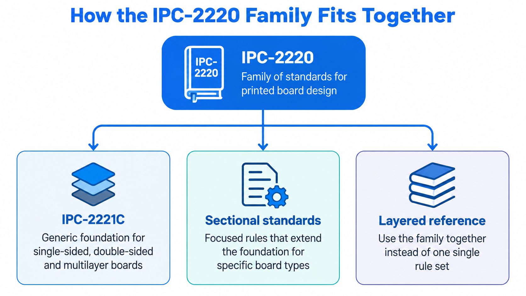
The IPC-2220 family is a layered reference system: IPC-2221C supplies the generic foundation, while sectional standards add requirements for particular board technologies. The IPC-2221C standard description identifies the relationship with rigid-board, flexible-board, and HDI design documents and highlights updated guidance affecting practical layout decisions.
The hierarchy below shows why the generic and sectional documents belong together.
<a id="establish-the-construction-record"></a>
Establish the construction record
Before routing begins, put these fields under revision control:
- Governing documents: Identify the generic and applicable sectional standards.
- Material system: Name the laminate construction and approval rules for substitutions.
- Copper construction: Identify foil and finished-copper expectations.
- Surface finish: Specify the intended finish rather than leaving it to purchasing.
- Via technology: Describe through, blind, buried, and microvia structures as applicable.
- Acceptance class: Establish the intended performance classification.
These fields prevent a common misunderstanding: the CAD file describes geometry, but it doesn't necessarily describe the complete manufacturing requirement. A drawn hole, for example, may need additional information about its finished condition and treatment.
<a id="review-the-stack-up-against-actual-functions"></a>
Review the stack-up against actual functions
IPC-2221C addresses material and copper-foil selection, edge plating, clearance, creepage, impedance tolerances, plane-clearance regions, feature-location tolerances, press-fit pins, and back-drilling. Turn those topics into a functional review:
- Verify insulation requirements. Check dielectric withstand, clearance, and creepage against the operating conditions. Clearance through air and creepage along a surface aren't interchangeable.
- Define controlled-impedance nets. Name the nets or routing classes, their targets, and permitted tolerances in the fabrication notes.
- Constrain back-drill stubs. Identify affected holes, drilling direction, and the acceptable remaining structure.
- Validate HDI construction. Confirm that the microvia arrangement and sequential-lamination plan match the intended implementation.
A press-fit connector deserves the same discipline. Its hole requirements come from the interaction between the pin specification and board construction, not merely a convenient drill selection.
Library rules also need clear boundaries. SMT land-pattern creation belongs under IPC-7351, while through-hole footprint requirements fall within IPC-2221 and IPC-2222. Record that distinction rather than allowing unrelated library conventions to blend unnoticed.
<a id="footprint-libraries-and-assembly-acceptance"></a>
Footprint Libraries and Assembly Acceptance
Every released footprint should identify its origin. Record the source standard, component package reference, and any deliberate departure in the library entry. A footprint that looks familiar in Altium or KiCad isn't necessarily suitable for the purchased component.
Use IPC-7351 when creating or auditing surface-mount land patterns. For through-hole parts, use the applicable IPC-2221 and IPC-2222 requirements alongside the component manufacturer's mechanical information. A mixed-technology assembly needs both approaches, not a single pad-generation rule applied indiscriminately.
<a id="audit-the-footprint-before-placement"></a>
Audit the footprint before placement
A reliable library-release sequence is:
- Pull from the controlled library. Avoid copying an unreviewed footprint from an unrelated project.
- Check the component datasheet. Verify package identity, terminal dimensions, pin numbering, orientation, and the recommended mounting information.
- Record the governing basis. Document the standard used and explain modifications such as altered pad geometry or assembly clearances.
- Confirm assembly acceptance. Establish the expected IPC-A-610 class and revision before releasing the assembly package.
The datasheet check matters because similar package names can hide different terminal arrangements or exposed-pad details. For a QFN, the electrical pad, solder-paste pattern, thermal vias, and inspection approach need coordinated decisions.
<a id="keep-footprint-design-separate-from-assembly-judgment"></a>
Keep footprint design separate from assembly judgment
IPC-A-610 concerns the acceptability of the assembled board. It isn't a substitute for defining the land pattern, assembly process, or inspection access. Name the required class and revision on the assembly documentation so the assembler and receiving inspector evaluate the same expectations.
Consider a BGA with vias beneath its pads. A usable land pattern alone doesn't settle via treatment, solder behavior, or inspection of hidden connections. The practical relationship between these decisions is explained in the BGA PCB assembly guide.
A footprint can be dimensionally correct and still create an assembly problem if the board construction and soldering process weren't reviewed together.
During DFM review, flag components that combine hidden joints, unusual terminal geometry, restricted rework access, or sensitive orientation. Provide the assembler with the actual component identity and assembly intent, not just a reference designator and an image of the package.
<a id="conductor-sizing-and-current-rules"></a>
Conductor Sizing and Current Rules
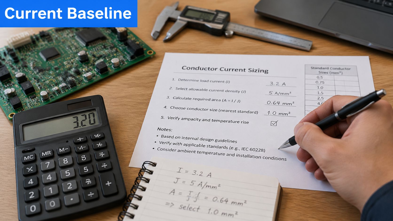
Size a conductor from its operating conditions, not from a remembered width-to-current shortcut. Use this sequence before committing the power routing:
- Set the load case. Establish continuous current, relevant transient behavior, ambient conditions, and design margin.
- Identify the conductor location. Distinguish external routing from internal routing.
- Select copper construction. Use the intended stack-up and finished-copper assumptions.
- Apply IPC-2152 guidance. Determine a suitable cross-section for the permitted temperature rise, using the applicable charts and conditions.
- Review heat paths. Examine nearby planes, pours, vias, restrictions, and heat-producing components.
- Validate demanding cases. Use thermal analysis and appropriate testing for high-current, metal-core, or tightly constrained constructions.
Keep the assumptions beside the calculation so another engineer can reproduce it.
<a id="why-the-chart-isnt-an-absolute-rating"></a>
Why the chart isn't an absolute rating
The commonly used external-trace chart descends from National Bureau of Standards work conducted from 1954 to 1956, while work from 1998 to 2000 clarified the absence of a similar public dataset for internal-conductor heating and helped motivate IPC-2152 development, as described by Printed Circuit Design & Fab.
The engineering consequence matters more than the history. Current capacity is a thermal result, not an intrinsic property of trace width alone. Copper thickness, conductor location, dielectric construction, board geometry, and the surrounding thermal environment all affect temperature rise.
Don't assume that an internal conductor always behaves like an external conductor with a simple correction factor. Its proximity to copper planes and the construction around it can change heat spreading. Likewise, a broad pour doesn't help equally if slots or narrow necks interrupt the useful thermal path.
For an additional conductor-sizing walkthrough, use the video below alongside the applicable standard and your construction assumptions.
<iframe width="100%" style="aspect-ratio: 16 / 9;" src="https://www.youtube.com/embed/OeV7SZ6-QyQ" frameborder="0" allow="autoplay; encrypted-media" allowfullscreen></iframe><a id="check-the-whole-power-path"></a>
Check the whole power path
Suppose a power rail meets the selected chart condition across most of its route. Near the load, it narrows between connector pads and passes beside a hot switching device. Inside the enclosure, the local ambient temperature is also higher than the calculation assumed.
The main trace can pass the initial calculation while the restricted segment exceeds the intended thermal limit. Review the narrowest copper, connection points, via transitions, and local heating, then revise the geometry or cooling assumptions.
Keep voltage-drop and fault-response checks separate from the temperature-rise calculation. A thermally acceptable conductor may still produce unacceptable supply loss, and normal-load sizing doesn't establish how the circuit behaves during a fault.
<a id="technology-specific-rules-for-flex-hdi-and-rf"></a>
Technology-Specific Rules for Flex, HDI and RF
Generic PCB design standards establish a foundation, but they don't remove the need to understand the manufacturing process. Technology-specific checks should follow the physical failure mechanism: bending fatigue, interconnect stress, electromagnetic discontinuity, or inadequate insulation.
<a id="flex-and-rigid-flex"></a>
Flex and rigid-flex
Under IPC-2223, review the bend geometry, routing through bending areas, coverlay, stiffeners, and copper selection. Distinguish a flex section installed into position from one that bends repeatedly during operation.
- Bending regions: Keep plated-through holes out of the active bend area as a conservative design practice, and avoid abrupt mechanical transitions.
- Copper and reinforcement: Select copper construction for the intended bending duty and place stiffeners with attention to where strain concentrates.
- Routing: Review trace direction, corners, and changes in conductor geometry through the bend.
For example, a connector stiffener can move the effective bending point toward an unsupported trace transition. A layout that fits the enclosure may still fail mechanically if the bend occurs somewhere other than the designer intended.
<a id="hdi-interconnects"></a>
HDI interconnects
IPC-2226 applies to the HDI construction, but the fabrication sequence must also be viable. Review microvia aspect ratio, stacked versus staggered arrangements, via-in-pad filling and planarization, and sequential lamination order. Evaluate back-drill stub requirements separately where the design includes drilled interconnects that need them.
A fine-pitch BGA escape may route cleanly in CAD while requiring a via stack that hasn't been approved for the intended construction. Define the structure before completing the escape, using the considerations in this HDI PCB manufacturer guide to organize the manufacturing discussion.
<a id="rf-and-high-speed-routing"></a>
RF and high-speed routing
Apply the generic design framework alongside material datasheets and electromagnetic analysis. Control impedance tolerance, preserve reference-plane continuity, and design ground-via fencing to suit the coplanar structure rather than copying spacing from an unrelated board.
A transmission line routed across a reference-plane interruption can create an unwanted return-path discontinuity even when its nominal width is correct. Specify test coupons that represent the intended routing structure and actual manufactured stack-up.
<a id="metal-core-and-ceramic-constructions"></a>
Metal-core and ceramic constructions
For metal-core boards, identify the dielectric thermal resistance, insulation requirement, and metal base material. A heat-spreading base doesn't eliminate the insulating layer between the circuit and that base; an unsuitable dielectric can undermine the intended thermal result.
Ceramic and other non-organic constructions need explicit scope checking. Don't assume that an organic-board sectional document fully defines their acceptance requirements.
- Substrate: Name the ceramic or other substrate and its required properties.
- Metallization: Identify the conductor system and relevant attachment interfaces.
- Verification: Agree on the inspection and test methods appropriate to the construction.
For example, a ceramic power substrate with an undefined metallization system leaves both assembly compatibility and acceptance ambiguous. Resolve those interfaces on the drawing rather than treating ceramic as a drop-in replacement for FR-4.
<a id="material-and-stack-up-choices-under-standards"></a>
Material and Stack-Up Choices Under Standards
The cheapest laminate can produce the more expensive product. If it reduces thermal margin, increases signal loss, or complicates future substitutions, the initial purchasing saving may disappear during validation or redesign.
Standards don't select the material for you. For high-speed and RF designs, evaluate dielectric constant, Dk, and dielectric loss, Df, across the operating frequency range, not just a catalog value, a distinction emphasized in the LCSC high-speed PCB design guide.
<a id="compare-materials-by-the-problem-they-solve"></a>
Compare materials by the problem they solve
| Material family | Useful starting application | Trade-off to resolve | |---|---|---| | Standard FR-4 | Cost-sensitive digital and lower-frequency circuitry | Confirm that electrical loss and thermal behavior meet the actual operating conditions. | | Low-loss hydrocarbon or PTFE-based laminates | RF and demanding high-speed paths | Balance electrical performance against fabrication requirements, availability, and substitution difficulty. | | Aluminum or copper metal-core | LED and power heat spreading | Evaluate the insulating dielectric and thermal interfaces, not just the metal base. | | Alumina or aluminum nitride ceramic | Applications requiring specialized thermal or RF behavior | Define metallization, attachment processes, mechanical constraints, and qualification evidence. | | Hybrid stack-ups | Designs combining demanding signal layers with cost-sensitive regions | Control material compatibility, construction, and approval of replacement materials. |
A low-loss laminate isn't automatically better for a simple controller. If the circuit doesn't need its electrical properties, the extra process constraints can create cost without solving a real problem.
Conversely, reducing layer count may force difficult return paths or remove useful thermal copper. Evaluate the complete design rather than treating layer count as an isolated purchasing target.
<a id="create-a-controlled-material-specification"></a>
Create a controlled material specification
Keep the following in a single revision-controlled specification:
- Electrical assumptions: Stack-up geometry, impedance targets, routing structures, and frequency-dependent material properties.
- Thermal limits: Operating conditions, heat-flow assumptions, and validation criteria.
- Substitution controls: Approved alternatives and the analysis or testing required before acceptance.
- Environmental constraints: Applicable chemical restrictions, recycled-content requirements, and supporting documentation.
- Test evidence: Material records, coupon results, and relevant electrical or thermal measurements.
For controlled structures, coordinate these requirements with the fabrication details described in the impedance-control PCB guide.
Surface finish belongs in the same decision process. Assembly compatibility, contact use, and required documentation can affect its suitability. Include factory data and lot traceability in the release requirements so a later investigation can connect measured performance to the material and process used.
<a id="acceptance-classes-and-handoff-to-fabrication"></a>
Acceptance Classes and Handoff to Fabrication
IPC Class 1, 2 and 3 by application and design impact
| Class | Typical Application | Design and Inspection Impact | |---|---|---| | Class 1 | General electronics where cosmetic imperfections carry less importance. | Less stringent acceptance in applicable areas; still specify finish, functionality, and required testing. | | Class 2 | Dedicated-service electronics requiring extended life and dependable operation. | Establish the applicable plating, construction, and inspection criteria; don't assume commercial use settles every requirement. | | Class 3 | High-reliability hardware where continued performance is critical, including mission-critical aerospace and life-support applications. | Review tighter applicable acceptance criteria and define the inspection evidence and qualification needed by the program. |
These are product-performance classifications, not a ranking of how advanced the circuit looks. A relatively simple controller can require high-reliability acceptance, while a dense commercial board doesn't become a higher-class product merely because it uses HDI.
The IPC-6012 qualification and performance standard covers rigid-board conductors, holes and vias, finishes and plating, test frequency, quality conformance, and electrical, mechanical, and environmental requirements. It also encompasses rigid constructions including blind and buried vias and metal-core boards.
<a id="turn-the-class-into-drawing-requirements"></a>
Turn the class into drawing requirements
The fabrication drawing should state:
- Governing acceptance: The required IPC-6012 revision and product class.
- Finished dimensions: Board thickness, tolerances, and relevant feature-location requirements.
- Copper and plating: Required finished conditions and applicable acceptance criteria.
- Finish: The surface finish and any selectively finished regions.
- Holes and vias: Finished-hole requirements, via treatment, and special processing.
- Electrical verification: Required test coverage, isolation requirements, and controlled-impedance testing where applicable.
- Qualification: Thermal or environmental testing required for the end product.
- Exceptions: Approved deviations, their scope, and the controlling authorization.
For high-reliability mission hardware, NASA GSFC guidance illustrates the use of a generic design foundation together with the relevant sectional standard, with impedance and isolation testing identified when required. The practical lesson is to specify the verification needed for the mission rather than assuming a class label defines every test.
<a id="understand-each-document-handoff"></a>
Understand each document handoff
Design to fabrication: IPC-2221 and the relevant sectional standard establish design requirements. IPC-6012 provides the rigid-board performance and qualification basis. The gap between them includes actual stack-up dimensions, registration capability, copper distribution, and the reliability of the selected via construction.
Fabrication to inspection: IPC-A-600 supplies bare-board visual acceptability criteria. Visual acceptance doesn't replace required electrical testing or qualification evidence, and a clean-looking board doesn't prove that its internal construction meets every requirement.
Board acceptance to product acceptance: Customer, product-safety, and regulatory requirements remain separate obligations. Passing the agreed PCB acceptance plan doesn't, by itself, qualify the finished medical device, industrial controller, or power supply.
Purchasing check: Require evidence against the actual drawing requirements, not a general statement that the factory follows IPC.
This is why nominal geometry checks can miss production risk. A trace may meet the layout rule while registration variation reduces the available annular ring. A via may have the intended CAD dimensions while the chosen construction requires additional reliability evidence.
<a id="resolve-capability-and-revisions-before-authorization"></a>
Resolve capability and revisions before authorization
IPC's explanation of connected design and production decisions emphasizes the relationship among design, DFM, materials, and packaging, and identifies the 2025 IPC-A-600M revision as an update involving imagery and expanded attention to HDI, microvia, and internal-defect inspection.
Name the required revision on the order. Don't assume that purchasing, engineering, and the supplier use identical editions, or that changing an edition is merely an administrative update.
For a prototype, define which results will support the production decision. For ongoing production, establish the required lot records, test reports, and change controls. A prototype supplier's successful build doesn't automatically qualify a different production construction.
Separate the final agreement into mandatory requirements, approved construction choices, and documented deviations. Give each deviation an owner and approval before manufacture; don't leave it buried in an email thread.
IPC compliant alone is not a purchasing specification. The drawing and order must identify what compliance means for that board and how the supplier will demonstrate it.
<a id="match-standards-to-your-product-before-quoting"></a>
Match Standards to Your Product Before Quoting
Standards and class by product context
| Product Context | Typical Class | Standards to Call Out | Extra Evidence to Request | |---|---|---|---| | Consumer electronics and IoT | Class 2 as a starting point, subject to product requirements | IPC-2221, applicable sectional standard, IPC-6012, IPC-A-600 | Stack-up, surface finish, and electrical test plan | | Industrial controls | Class 2 unless operational risk requires otherwise | IPC-2221, IPC-2152, IPC-6012, applicable sectional standard | Thermal review and current-carrying trace calculations | | Automotive electronics | Customer-specified Class 2 or Class 3 | IPC-2221, IPC-6012, customer qualification requirements | Supplier quality-system evidence and lot traceability | | Medical devices | Class 2 or Class 3 according to risk and customer requirements | IPC-2221, IPC-6012, IPC-A-600, customer requirements | Quality-system evidence and controlled regulatory documentation | | Aerospace and military | Class 3 where required by the program | IPC-2221 plus applicable sectional standard and production specification | Impedance and isolation test requirements, qualification coupons | | LED lighting and power | Class 2 as a starting point, with thermal review | IPC-2152, IPC-6012 for applicable rigid or metal-core construction | Thermal-resistance information and copper construction | | RF, microwave, and 5G | Class 2 or Class 3 according to program requirements | IPC-2221, applicable sectional rules, material datasheets | Dk and Df across the operating range and measured impedance |
Treat these entries as quoting starting points, not automatic classifications. The customer's requirements and consequences of failure determine the final selection. Industry names alone don't establish a complete acceptance specification.
<a id="prepare-a-quote-ready-package"></a>
Prepare a quote-ready package
Attach the fabrication and assembly drawings to the manufacturing files. Include the standards revisions, class, proposed stack-up, impedance requirements, power-copper construction, finish, test coverage, and approved deviations. RF and metal-core projects also need the material and thermal information necessary to evaluate the proposed construction.
For an assembly quotation, export the Gerber, BOM, and pick-and-place files. Native files can help resolve design questions; we accept Altium, Eagle, KiCad, and PADS files for DFM review.
Use consistent revision identifiers across the package. A current Gerber set paired with an older BOM or assembly drawing creates an avoidable authorization problem, even if each file opens correctly.
<a id="know-what-happens-after-submission"></a>
Know what happens after submission
Our quotation process follows this sequence:
- Upload the files through the secure portal, including Gerber, BOM, and pick-and-place information.
- Receive engineering review of the design and component availability, with DFM feedback.
- Review the quotation with transparent pricing and lead-time options.
- Authorize production, after which the boards are manufactured, assembled, tested, and shipped worldwide.
We manufacture every board to IPC Class 2 or Class 3 standards, with 100% AOI, flying-probe, and electrical testing. Your order still needs to identify any additional program-specific inspection, qualification, and reporting requirements.
Before authorization, reconcile the quotation with the drawing. Check that material substitutions, inspection coverage, and requested reports are included rather than assumed.
Send the standards package with the design files before requesting the first quote. That gives engineering a defined target and makes competing quotations easier to compare on construction and evidence, not just price.
Lianyuhong Technology Co.,Ltd offers PCB design, fabrication, and turnkey assembly with engineering DFM review to connect your standards requirements to a manufacturable release. Visit Lianyuhong Technology Co.,Ltd and submit your design files together with the required IPC revisions, acceptance class, stack-up, and test plan for review and quotation.