
Popular advice often says that a BGA assembly is good if its X-ray image looks acceptable. That's a useful first check, not proof that every hidden joint will survive the product's service life. A joint's location, the package's warpage, the board design and the product's temperature changes all affect the result.
A sound bga pcb assembly process connects design choices to paste printing, reflow, inspection and reliability testing. The key is to know what each check can reveal, and when an X-ray result needs more evidence before engineering can accept the board.
Table of Contents
- What BGA PCB Assembly Is and How It Differs from Through-Hole
- BGA Pitch, Ball Size and Tolerances at a Glance
- PCB Design Rules That Prevent Assembly Trouble
- How BGA Assembly Runs From Package to Reflow
- Stencil and Reflow Settings That Set Joint Quality
- Inspection, Acceptance and Defect Root Causes
- Planning a BGA Build From Prototype to Production
<a id="what-bga-pcb-assembly-is-and-how-it-differs-from-through-hole"></a>
What BGA PCB Assembly Is and How It Differs from Through-Hole
Think of a through-hole part as a letter pushed through a slot: its leads pass through the PCB, and the soldered ends are visible on the other side. A BGA is more like an apartment block whose doors all open onto the basement floor. Its connections are a grid of solder balls on the underside, hidden once the package is mounted.
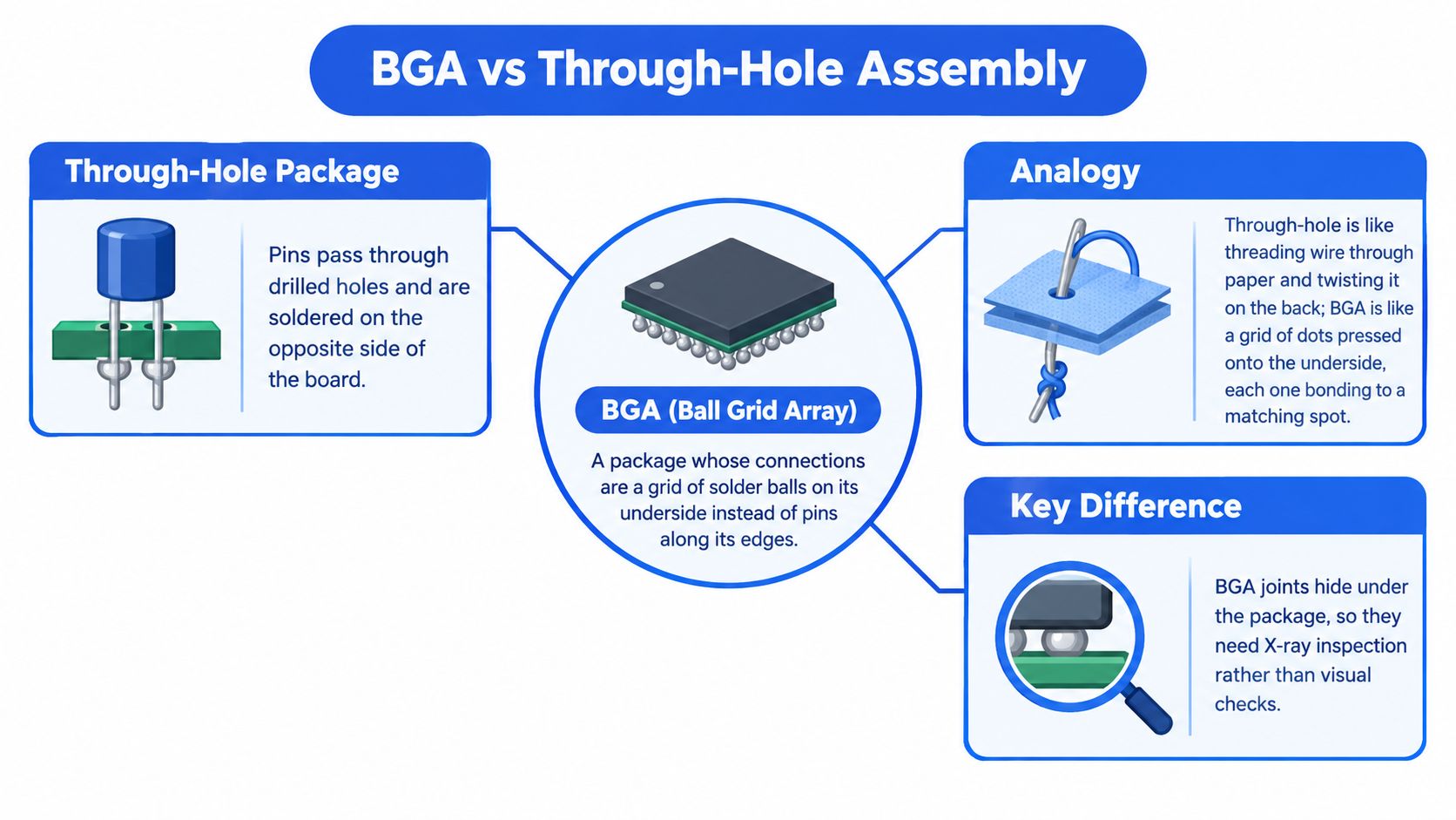
During assembly, solder paste is printed onto PCB pads and the BGA is placed over them. In the reflow oven, the paste and balls melt; surface tension helps each ball form a joint with its corresponding pad. The board therefore relies on an array of connections that can't be inspected directly from above.
Package families include plastic BGA (PBGA), which uses a plastic substrate; ceramic BGA (CBGA), which uses a ceramic package; and tape BGA (TBGA), which uses a tape-based substrate. Package construction matters because it affects the way the package and board respond to heat.
<a id="bga-and-through-hole-on-the-same-board"></a>
BGA and through-hole on the same board
Through-hole technology (THT) uses drilled holes and soldered leads, often assembled with wave or selective soldering. BGA uses surface pads and reflow. Many products combine them: a processor might be a BGA, while its board uses through-hole connectors or power components.
BGA allows connections across the underside of a package, supporting higher connection density, shorter interconnects and smaller footprints than edge-lead packages may allow. The trade-off is that every solder joint sits beneath the package. Optical inspection can't verify the array, so production relies on other controls, including X-ray inspection.
The reliability risk doesn't disappear when a board passes electrical test. NASA's BGA selection guidelines report typical joint lifetimes from approximately 100 to about 6,000 thermal cycles for assemblies exposed to temperatures between −55°C and 100°C. The guidance says thermal cycling, coefficient-of-thermal-expansion mismatch, mechanical bending and PCB warpage govern joint reliability; larger temperature swings generally shorten life. Initial electrical continuity is a snapshot, not evidence that a joint will last through the product's service conditions.
<a id="bga-pitch-ball-size-and-tolerances-at-a-glance"></a>
BGA Pitch, Ball Size and Tolerances at a Glance
Pitch is the distance from the center of one solder ball to the center of the next. It controls how much margin the assembly line has for printing paste, placing the part and routing signals out of the array. Everything else follows from it.
| Pitch | Assembly difficulty | |---|---| | 0.80 mm | Paste volume and stencil-aperture design decide yield | | 0.65 mm | Fine pitch; laser-cut stencil and SPI expected | | 0.35 mm | Advanced HDI; confirm capability with the provider |
Ball and pad diameters are left off this table for a reason. Two packages at the same pitch can use different ball sizes and land patterns, so those dimensions, and their tolerances, must come from the package datasheet rather than being inferred from pitch. The datasheet is also where coplanarity limits and the recommended land pattern live.
Read each row as a signal about the process. At 0.80 mm pitch, paste volume and aperture design decide whether joints form consistently. As pitch tightens, errors in print quality and placement alignment have less room to be absorbed.
<a id="when-the-process-needs-tighter-control"></a>
When the process needs tighter control
At 0.65 mm pitch, fine-pitch printing calls for a laser-cut stencil and solder-paste inspection (SPI) to check the deposit before placement. Tight routing may also push the board toward an HDI escape strategy. At 0.35 mm pitch, confirm that the fabricator's board construction and the assembler's process support the design rather than assuming every line can handle it.
Lianyuhong can assemble components as small as 01005 and BGA devices down to 0.35 mm pitch. That helps when a design sits near the tight end of standard practice, but the package drawing, routing, stencil and inspection plan still need to work together.
Tolerances tighten again at inspection. A void covering roughly 25% of a joint's measured area can be acceptable on an interior ball where mechanical stress is low. The same void at a corner joint, which sees the most strain during thermal cycling, is a different story. For high-risk builds, a flat X-ray pass or fail is a weak acceptance criterion; ask whether the plan includes 3D CT, a destructive cross-section on a sample, or thermal cycling to prove the joint.
Before approving an assembly drawing, check pitch, ball diameter and array size. Those three details let the layout and assembly teams confirm the land pattern, routing space and inspection approach.
<a id="pcb-design-rules-that-prevent-assembly-trouble"></a>
PCB Design Rules That Prevent Assembly Trouble
A successful BGA footprint starts with the joint geometry, then accounts for routing and heat. Pad type, via treatment, soldermask registration and board warpage all influence how reliably solder connects the package to the board.
<a id="choose-pads-and-vias-for-the-actual-pitch"></a>
Choose pads and vias for the actual pitch
With non-solder-mask-defined (NSMD) pads, copper is smaller than the soldermask opening, so the copper edge defines the pad. This often gives the joint a consistent geometry. With solder-mask-defined (SMD) pads, the mask opening defines the joint boundary. SMD can be useful at fine pitch, but it relies on accurate soldermask registration.
A via-in-pad can give the router an escape path when there's little room between balls. For tight layouts, it needs to be filled and capped; an open via can wick solder away from the joint. Dogbone fanout uses a short trace from the pad to a nearby via, with the trace and via sized for the pitch and board fabrication capability. Tight arrays may also need soldermask dams between adjacent pads, provided the fabricator can reliably hold them.
<a id="manage-heat-and-board-shape"></a>
Manage heat and board shape
A thermal relief connects a ground pad to a plane through narrow copper spokes. Those spokes reduce heat sinking, helping the joint reach reflow temperature. High-current power pads may need a solid plane connection instead, so the electrical and thermal requirements must be weighed together.
For controlled-impedance signals, work from a documented stack-up and confirm routing geometry with the fabricator. Large BGAs also need attention to copper balance, board thickness and any required stiffeners. Uneven copper or board flex can increase warpage and concentrate strain near the package perimeter.
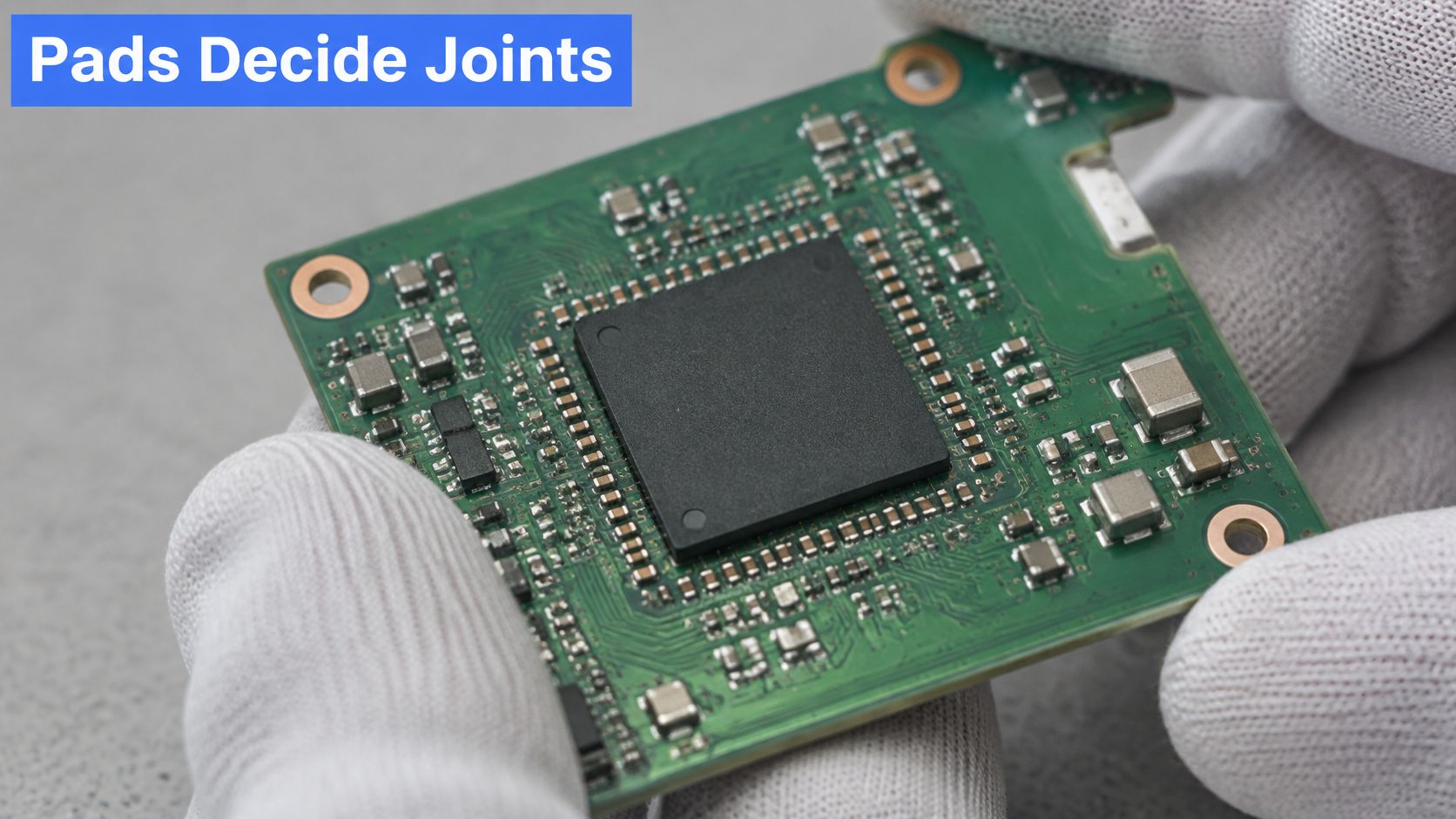
NIST's accelerated testing of lead-free assemblies included temperature ranges from −40°C to 125°C and 0°C to 100°C, with minimum five-minute dwells at the extremes. The reported lead-free combinations performed equivalently to or better than the tin-lead benchmark in those tests. That finding doesn't make alloy selection a stand-alone reliability decision: pad geometry, ball size, PCB thickness, copper distribution, component warpage and reflow uniformity all affect the strain on each joint.
Design rule: Review the BGA escape routing, board stack-up and expected warpage before release, not after a failed assembly points back to the layout.
For a design that needs a fresh review, Lianyuhong's PCB layout and design service includes layout, signal and power integrity simulation, and DFM review. A DFM check can flag land-pattern or routing problems before fabrication.
<a id="how-bga-assembly-runs-from-package-to-reflow"></a>
How BGA Assembly Runs From Package to Reflow
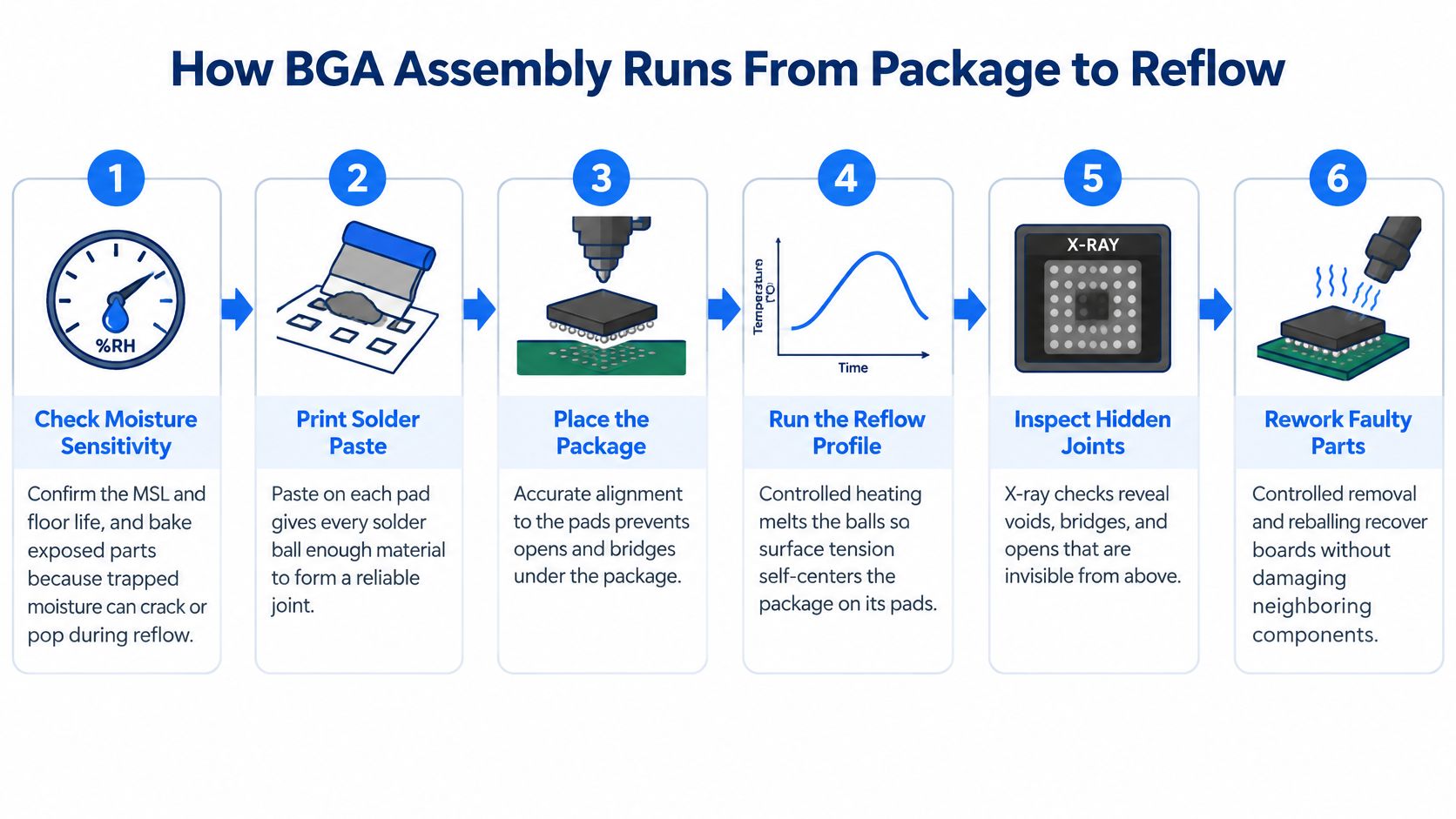
A dependable build depends on the steps before and after the oven, not just the reflow profile. Each check catches a different risk, from moisture in a package to hidden defects beneath the finished component.
-
Check moisture sensitivity. Confirm the package's moisture sensitivity level (MSL) and floor life, then bake parts when handling records or exposure indicate they need it. Moisture trapped inside a package can cause damage during reflow.
-
Prepare the PCB. Check board flatness and pad finish, and bake a bare board if moisture exposure calls for it. A flat surface and solderable pads help the balls meet their intended lands.
-
Inspect the package. Check for damaged or missing balls and signs of coplanarity trouble. A damaged ball or uneven package can leave a connection incomplete after reflow.
-
Print solder paste. Use a laser-cut stencil to deposit paste onto each pad. The paste supplies solder to help form the BGA joints.
-
Run SPI. Inspect paste volume and offset before placement. Correcting a print problem here is easier than diagnosing a hidden open or bridge after reflow.
-
Place the BGA. A vision-guided placement system aligns the package to the pads. As the solder melts, surface tension helps center the balls, but it can't correct a poor print or a damaged package.
-
Reflow the assembly. Use a validated profile matched to the paste, board and component. Nitrogen reflow is an available process at Lianyuhong; a controlled profile matters more than assuming one oven recipe suits every BGA.
-
Inspect the joints. Automated optical inspection (AOI) can find visible surface issues, while X-ray checks hidden connections. Neither replaces process records or any reliability tests required by the product.
-
Apply underfill when the application calls for it. Capillary underfill is dispensed after reflow and wicks beneath the package; no-flow underfill is applied before placement and cures during reflow. Confirm fill with X-ray or cross-section, and plan rework in advance because removal requires heat before the BGA can be replaced.
-
Complete mixed assembly and test. Add through-hole parts using wave or selective soldering, then run the functional test defined for the board. Lianyuhong's assembly capabilities include nitrogen reflow, wave and selective soldering, SMT from 01005, BGA from 0.35 mm pitch, and through-hole assembly for connectors and power parts.
The process below shows the main checkpoints from incoming package handling through inspection and repair.
<iframe width="100%" style="aspect-ratio: 16 / 9;" src="https://www.youtube.com/embed/_E_q1xIkD8o" frameborder="0" allow="autoplay; encrypted-media" allowfullscreen></iframe><a id="stencil-and-reflow-settings-that-set-joint-quality"></a>
Stencil and Reflow Settings That Set Joint Quality
| Setting | Typical target | What it controls | |---|---|---| | Preheat ramp | 1 to 3 °C per second | Thermal shock and solvent outgassing | | Peak temperature | Set from the solder-paste and component specifications | Complete ball collapse without package damage | | Cooling ramp | 4 °C per second or less | Grain structure and residual stress | | Stencil thickness | Select for the pitch and paste-volume requirement | Paste volume per joint |
A thermal profile has to heat the whole assembly in a controlled way. Treat these targets as starting points for process development, not as settings to copy without checking the solder-paste and component requirements.
<a id="what-each-zone-does"></a>
What each zone does
Preheat controls how quickly the board warms. A controlled ramp limits thermal shock and gives solvents a chance to leave the paste. During soak, flux works on the pad surfaces and the board evens out in temperature. This matters on large packages because cooler regions can lag behind warmer ones.
Time above liquidus is the interval when solder is hot enough to wet and form a joint. For SAC305, the planning reference is 217°C; confirm the paste manufacturer's profile and the package's thermal limits before setting the production recipe. Peak temperature must be high enough for full ball collapse but not so high that it damages the package or board.
Stencil thickness controls paste volume, so don't choose it in isolation from pitch and aperture design. Fine-pitch BGA work commonly uses 0.10 to 0.12 mm stencil thickness, with an aperture-to-pad ratio near 1:1 as a starting point. A large package may need corner aperture reductions to control bridging. Lianyuhong's SMT stencil guidance can support decisions about stencil fabrication and aperture design.
<a id="measure-the-package-not-just-the-oven"></a>
Measure the package, not just the oven
For a large BGA, attach thermocouples at locations expected to run hottest and coolest. The oven's display reports zone settings, not necessarily the temperature at every solder joint. Package warpage near peak temperature can lift the body away from paste and contribute to head-in-pillow defects or uneven solder collapse.
Change one process variable at a time. After each change, check the joints with X-ray; use a cross-section when the image can't settle a critical question about the joint interface.
<a id="inspection-acceptance-and-defect-root-causes"></a>
Inspection, Acceptance and Defect Root Causes
A clean X-ray image doesn't automatically mean a board is reliable. It means the chosen inspection method didn't reveal a disqualifying defect under its criteria. Acceptance still needs to reflect the joint's position, void geometry, package and product environment.
<a id="build-an-inspection-stack"></a>
Build an inspection stack
SPI checks paste volume and offset before the package is placed. AOI can detect visible faults such as component misalignment, but it can't see the solder balls under a BGA. After reflow, transmission or oblique X-ray can reveal hidden bridging, opens and voids; 3D CT may help when a 2D projection can't resolve a three-dimensional feature.
X-ray is a screening tool, not a substitute for every other test. A cross-section removes and cuts through a sample to examine the joint directly, so it can validate inspection criteria but won't preserve that sample for use. Flying probe can locate opens and shorts without a dedicated fixture, while functional test checks whether the assembled product works as intended.
Texas Instruments' lead-free BGA application note recommends transmission X-ray sampling after reflow to identify bridging, shorts, opens and voids. The same note summarizes an IPC-cited study in which voiding below 25% of a solder joint's area generally showed no adverse effect on measured reliability. It also cites a stricter 9% maximum criterion for IPC Class 3 BGA guidance. These are different acceptance frameworks, not interchangeable guarantees.
<a id="why-a-void-percentage-alone-can-mislead"></a>
Why a void percentage alone can mislead
The peer-reviewed BGA thermal-cycle study cycled samples between −20°C and +125°C, with 15-minute dwells at each extreme. After 2,325 hours, researchers used X-ray analysis, and the fitted characteristic life was 4,184 cycles. Outer-ring joints had lower thermal-fatigue reliability than inner-ring joints, while void effects varied with location and size.
That study also reports that IPC-A-610E limits a void to no more than 30% of an individual solder ball's projected area in the cited acceptance framework. A void above a critical volume could cause an inner-ring joint to fail before an outer-ring joint. Separately, the Texas Instruments note describes a reliability study that measured approximately 10% lower bond strength with 6–10% interfacial voiding. A void near an interface may matter more than a larger void in a less critical part of a joint.
So when is a 25% void acceptable? Only when the applicable acceptance criteria, void position, joint function and product service conditions support that decision. If the BGA carries a critical signal or sits in a high-stress thermal area, or if a 2D projection leaves uncertainty about the void shape, engineering may need 3D CT, a destructive cross-section, thermal cycling or electrical stress testing. For a lower-risk design, documented X-ray criteria and process controls may be enough. The product team should state the rationale rather than treating one percentage as proof of reliability.
<a id="diagnose-the-defect-before-changing-the-process"></a>
Diagnose the defect before changing the process
| Symptom | Likely root cause | How to confirm | Fix | |---|---|---|---| | Head-in-pillow | Ball and paste fail to fuse as warpage lifts the package, or balls are oxidized | Oblique X-ray; warpage check at peak temperature | Reduce warpage with bake, stiffeners or panel support; verify profile; check ball condition | | Solder bridging | Excess paste, smeared stencil or offset placement | X-ray and AOI on perimeter rows | Reduce aperture, clean stencil, calibrate placement vision | | Excess voiding | Flux outgassing, oxidized paste, short soak or unfilled via-in-pad | X-ray void area and location per joint | Longer soak, nitrogen, vacuum reflow, filled and capped vias | | Open joint | Insufficient paste, coplanarity fault or pad oxidation | SPI volume data, X-ray, flying probe or functional test | Check paste volume, enforce coplanarity limits, review pad finish | | Tombstoning near passives | Unequal pad heating or paste on one pad only | AOI and visual inspection | Balance pad sizes and paste, review thermal relief | | Pad cratering | Board flex or high-stress reflow fractures the pad or laminate | Cross-section showing cracks at the pad | Reduce flex, stiffen the board, review pad and laminate design |
Use defect distribution to narrow the investigation. Faults concentrated along one edge point toward package or board warpage, or stencil alignment; defects spread across the array point more toward the paste or reflow profile. Tombstoning in nearby passives calls for a check of uneven pad heating.
Lianyuhong performs incoming material inspection and AOI, X-ray and flying-probe testing on every PCB. For high-risk products, the escalation plan should classify voids by size and location, then use cross-sections or reliability testing to validate the inspection criteria where needed. Rejecting every void wastes usable product; accepting every void under a single area limit can miss a meaningful reliability risk.
<a id="planning-a-bga-build-from-prototype-to-production"></a>
Planning a BGA Build From Prototype to Production
Good build planning starts with complete files and a clear test plan. Before buying parts, give the assembly team enough information to check whether the footprint, components and process are compatible.
Lianyuhong's process follows four steps: upload the Gerber files, BOM and pick-and-place data through a secure portal; engineers review design and component availability and return DFM feedback; you receive a detailed quotation with pricing and lead-time options; then the boards are fabricated, assembled, tested and shipped worldwide. A prototype assembly overview can help teams prepare for an initial build.
<a id="prepare-the-build-package"></a>
Prepare the build package
- Confirm package details. Include the manufacturer's part number and package drawing so the team can verify the pitch, array and land pattern.
- Check component availability. BGA parts can be the long-lead item, so confirm stock before committing to a schedule.
- Supply assembly files. Provide current Gerbers, BOM and pick-and-place coordinates, plus assembly drawings and any special handling instructions.
- Define acceptance and tests. State the applicable IPC class, X-ray coverage, traceability needs, functional test requirements and rework expectations.
Turnkey assembly at Lianyuhong has no minimum order quantity and supports prototype through production. For a consigned full kit, the customer supplies the boards and components, while Lianyuhong performs SMT and through-hole assembly and keeps assembly records. The fastest stated turnaround for turnkey PCB assembly is 24 hours, but that doesn't remove the need to confirm material availability and the project's actual lead time.
<a id="ask-about-evidence-not-just-equipment"></a>
Ask about evidence, not just equipment
Before approving a build, clarify whether X-ray is performed on every board or sampled, and whether 3D CT is available if a 2D image can't resolve a defect. Ask how reflow profiles and lot records are retained, which acceptance class applies, and how the team handles BGA rework. A machine list matters less than an agreed inspection and escalation plan.
Send the design files for a DFM check before purchasing components. That gives the engineering team a chance to flag routing, land-pattern or process concerns while the design can still be changed.
For BGA projects, Lianyuhong Technology Co.,Ltd offers PCB fabrication and turnkey SMT, through-hole and mixed-technology assembly, with X-ray inspection and support for BGA pitches down to 0.35 mm. Share your files and build requirements with Lianyuhong Technology Co.,Ltd to start a DFM review before production.