
Your LED driver works on the bench. Then it runs for an hour, the case gets hot, and the output starts to drift. You've added copper pours and vias to your FR-4 board, but the heat still has nowhere useful to go.
That's usually when a ceramic board enters the conversation. Not because ceramic sounds premium, but because the substrate itself becomes part of your thermal design.
Table of Contents
- What Ceramic PCBs Are and Where They Fit
- Choosing Between Al2O3 and AlN Substrates
- Comparing DBC, DPC, Thick-Film and LTCC Processes
- Designing and Assembling Ceramic Boards Without Surprises
- Testing Thermal Cycling and Verifying Reliability
- Evaluating Cost, Lead Times and Certifications
- Questions to Ask Your Ceramic PCB Supplier and Next Steps
<a id="what-ceramic-pcbs-are-and-where-they-fit"></a>
What Ceramic PCBs Are and Where They Fit
Think of a standard laminate board as a plastic tray that holds copper tracks. It insulates well enough, but it's a poor heat path. A ceramic PCB replaces that tray with a ceramic plate. That plate does three jobs at once. It electrically insulates the circuit, it mechanically supports components, and it moves heat away from hot devices.
That difference matters when you mount power semiconductors, high brightness LEDs, or dense RF parts. The copper pattern still carries current, but the ceramic underneath decides how hot the device gets and how much stress builds up when temperature swings.
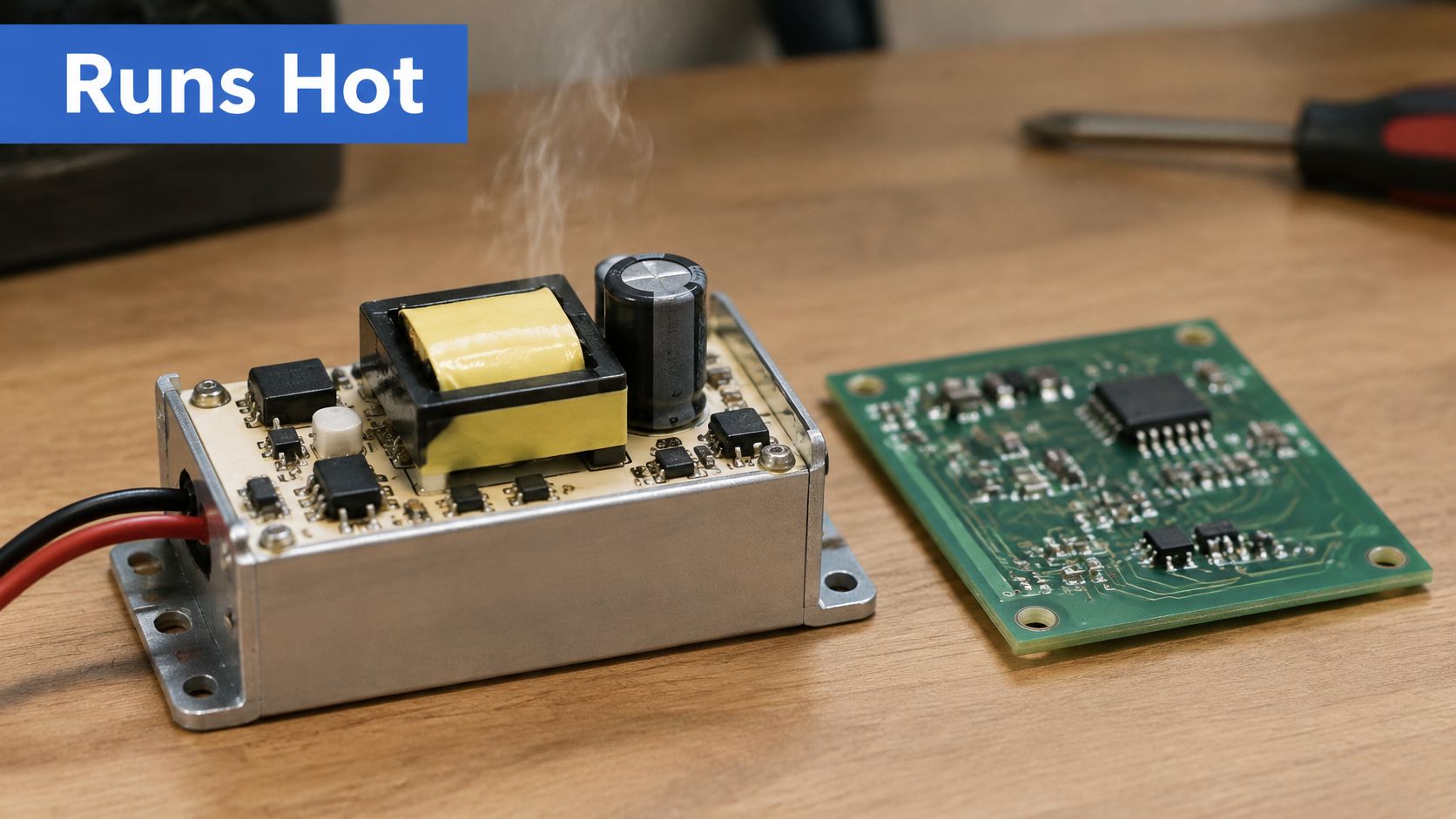
Here's a failed power unit that shows why teams stop treating the board as a passive carrier.
<a id="where-engineers-reach-for-ceramic"></a>
Where Engineers Reach for Ceramic
You'll see ceramic substrates most often in a few families:
- Power modules and inverters: Thick copper carries high current while the ceramic isolates that copper from a heatsink.
- Industrial drives and converters: Repeated heating and cooling punish weaker laminates.
- LED power systems: Heat leaves the diode through the substrate instead of cooking the board.
- RF and sensor packages: Stable dimensions and controlled electrical properties matter more than low laminate cost.
Not every hot board needs ceramic. If heat is moderate and spread over a large area, a metal core PCB option for thermal management may solve the problem at lower cost. Ceramic earns its place when you need electrical isolation, high temperature tolerance, and a compact heat path in the same part.
The technology isn't new. In 1975, Burgess and Sun first used the gas metal eutectic method to bond copper foil to ceramic at high temperature, forming a copper, copper oxide and ceramic joint without a conventional polymer adhesive, as described in historical technical literature on direct bonded copper development. Toshiba later applied that approach to semiconductor power modules, and it became a standard base for power multichip modules. That's why a capable Ceramic PCB manufacturer is usually judged first on substrate and bonding, not on fancy solder mask options.
<a id="choosing-between-al2o3-and-aln-substrates"></a>
Choosing Between Al2O3 and AlN Substrates
Most buying conversations start with two materials. Alumina, or Al2O3, is the workhorse. Aluminum nitride, or AlN, is the high performance option. The wrong way to choose is to pick the bigger conductivity number and move on.
Alumina has a thermal conductivity of roughly 24 to 28 W/mK, while typical AlN is about 170 W/mK, which means AlN provides approximately six to seven times the heat conduction capability under those cited values, according to a historical account of ceramic substrate development and DBC milestones. That gap is real. It doesn't mean every design runs six times cooler, because your die attach, copper, baseplate, and airflow also resist heat flow.
<a id="ceramic-substrate-options-at-a-glance"></a>
Ceramic Substrate Options at a Glance
| Substrate | Typical thermal conductivity | Best-fit application | |---|---|---| | Al2O3 (alumina) | 24 to 28 W/mK | Cost sensitive power, LED, and thick film circuits with moderate heat | | AlN (aluminum nitride) | About 170 W/mK | High power density modules where compact heat removal justifies cost | | Si3N4 (silicon nitride) | Discussed for DBC power use, confirm grade data with supplier | Demanding power cycling applications where mechanical toughness matters |
History explains the split. Alumina DBC reached an industrial milestone in 1983, when curamik electronics became the first company reported to produce DBC alumina substrates on large panels at an affordable cost, as noted in that same historical account. AlN gained ground as a preferred alternative to beryllium oxide because of toxicity concerns. Safer did not mean simpler.
Practical rule: Buy AlN for a proven thermal bottleneck in the substrate, not for a datasheet trophy.
Copper bonding to AlN is harder than bonding to alumina. Your supplier may need specialized surface treatment or active brazing. Adhesion isn't a vague promise, either. Patent documentation from 1995 records a copper film peel strength of 14 lb/in for a 5 mil copper film on AlN using that approach. Ask what adhesion evidence your supplier will provide for your exact copper thickness.
Use alumina when heat load is moderate, board area gives you spreading room, and cost pressure is real. Use AlN when power density is high, space is tight, or a lower junction temperature protects lifetime. If you can't show where heat gets stuck in your stack, you aren't ready to pay for AlN.
<a id="comparing-dbc-dpc-thick-film-and-ltcc-processes"></a>
Comparing DBC, DPC, Thick-Film and LTCC Processes
Substrate choice tells you what the plate is. Process choice tells you how copper or conductors get onto it. Suppliers quote very different jobs under the same ceramic label, so you need to separate these routes clearly.
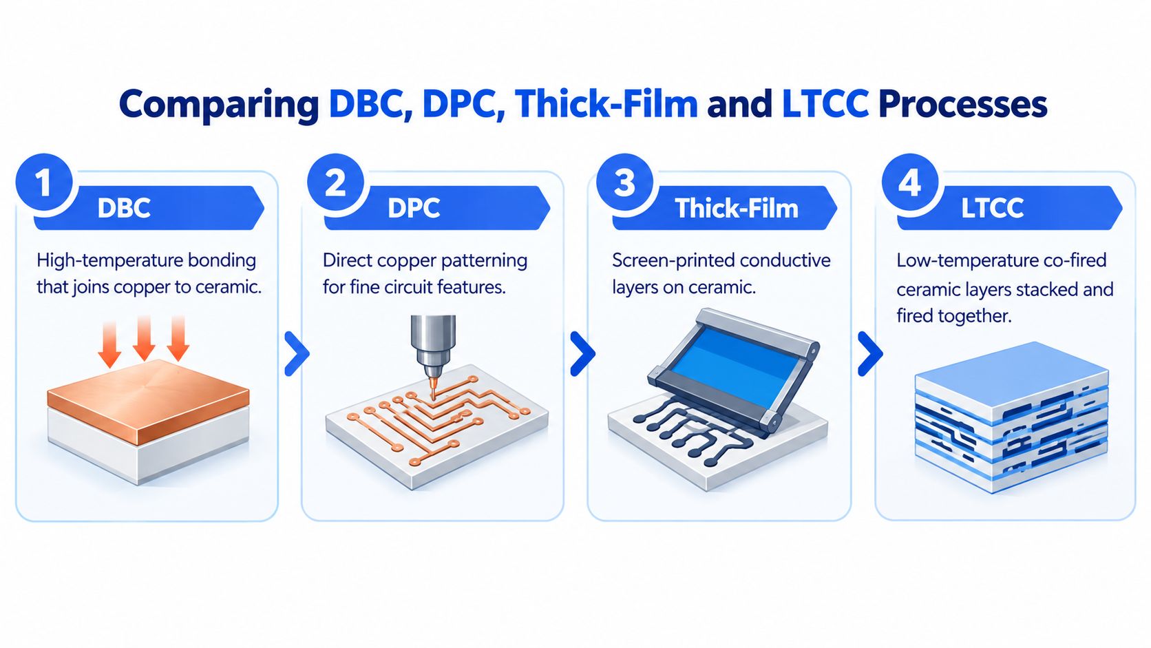
The diagram below sets the four common routes side by side before you compare quotes.
<a id="how-each-route-is-built"></a>
How Each Route Is Built
Direct bonded copper, or DBC, bonds copper foil to fired ceramic at high temperature, then patterns the copper. On alumina, bonding depends on copper oxide interdiffusion and formation of copper aluminate at approximately 1,065°C. Published characterization reports DBC bonding above 1,000°C to Al2O3, AlN, or Si3N4, with dielectric strength near 20,000 V/mm and a broad thermal conductivity range of approximately 24 to 180 W/m·K, as detailed in published technical characterization of DBC substrates for power electronics. That's why DBC suits thick copper power circuits.
Direct plated copper, or DPC, starts with a deposited seed layer and builds copper by plating. Engineers evaluate it when they need finer features or plated structures that etched DBC foil can't deliver cleanly. Don't treat it like FR-4 plating moved onto ceramic. Confirm finished line and space, copper build, and via construction in writing.
Thick film screens conductive paste onto ceramic and fires it. It's useful for durable conductors and, in some designs, printed resistors or other functional pastes. Features are coarser than plated routes, and results depend heavily on paste, screen, and firing profile.
LTCC, or low temperature co-fired ceramic, stacks patterned ceramic tapes and fires them together into a multilayer body. That fits integrated packages and cavities, but shrinkage and layer registration become central risks. A supplier offering DBC and thick film on Al2O3 and AlN doesn't automatically offer LTCC, so confirm that capability directly.
Watch this short process overview, then map each step to your own copper thickness and geometry needs.
<iframe width="100%" style="aspect-ratio: 16 / 9;" src="https://www.youtube.com/embed/x5OlTcqB6U8" frameborder="0" allow="autoplay; encrypted-media" allowfullscreen></iframe>Don't accept generic tolerance claims. Request finished copper thickness, minimum trace and gap after etching or plating, ceramic thickness tolerance, flatness, and surface finish for your artwork revision.
<a id="designing-and-assembling-ceramic-boards-without-surprises"></a>
Designing and Assembling Ceramic Boards Without Surprises
Many ceramic failures don't start as a dramatic crack through the middle of the plate. They start at a copper edge.
Copper and ceramic expand at different rates. During thermal cycling, tensile stress concentrates at trace edges. Those stresses can initiate conchoidal fractures that run parallel to the substrate surface and cause trace delamination. Thick copper helps current capacity, but it also adds mechanical force at those edges.
<a id="design-controls-that-reduce-edge-stress"></a>
Design Controls That Reduce Edge Stress
- Control copper geometry: Avoid unnecessary copper mass near vulnerable edges and sharp features that concentrate stress.
- Add edge relief where suitable: Small geometry changes can reduce peak stress, but your supplier must confirm the finished etched shape.
- Simulate before layout freeze: Thermal mechanical simulation is cheaper than learning from cracked prototypes.
- Share the mission profile: Give operating temperature range, cycle profile, and mounting method before quoting, not after.
Reducing copper mass near vulnerable edges has been reported to significantly improve cycling reliability. That trade is plain. You may give up some copper area to gain life.
A proper PCB layout review before fabrication should catch isolation gaps, pad geometry, and assembly land issues while they're still drawing changes. Ask for a written DFM response that lists approved assumptions and deviations.
A clean copper pattern doesn't prove a sound copper to ceramic bond. Ask how hidden interfaces will be checked.
Assembly adds its own risks. Solder joints, die attach, stencil apertures, and mounting pressure can stress a substrate that passed bare board inspection. Fine pitch and hidden joints raise yield risk, so your process plan should name solder paste inspection, automated optical inspection, and X-ray where the joint type justifies them. A DFM and BOM review on every order helps catch footprint, stencil, and component availability problems early, before ceramic panels are committed.
Before you release files, confirm ceramic grade and thickness, copper on one or both sides, finished trace geometry, hole or via construction, flatness datum, surface finish, and singulation method. Ceramic doesn't forgive vague drawings.
<a id="testing-thermal-cycling-and-verifying-reliability"></a>
Testing Thermal Cycling and Verifying Reliability
A supplier tells you a board passed thousands of thermal cycles. Your next question should be simple. Passed what, exactly?
Cycle count alone proves little. Standards such as IEC 60068-2-14 and JEDEC JESD22-A104 define test methods, not a universal pass or fail cycle count for your product. That distinction is explained in guidance on ceramic PCB thermal cycling tests at 150°C. You still have to define the test object, temperatures, ramp rate, dwell time, sample size, inspection intervals, and failure criteria.
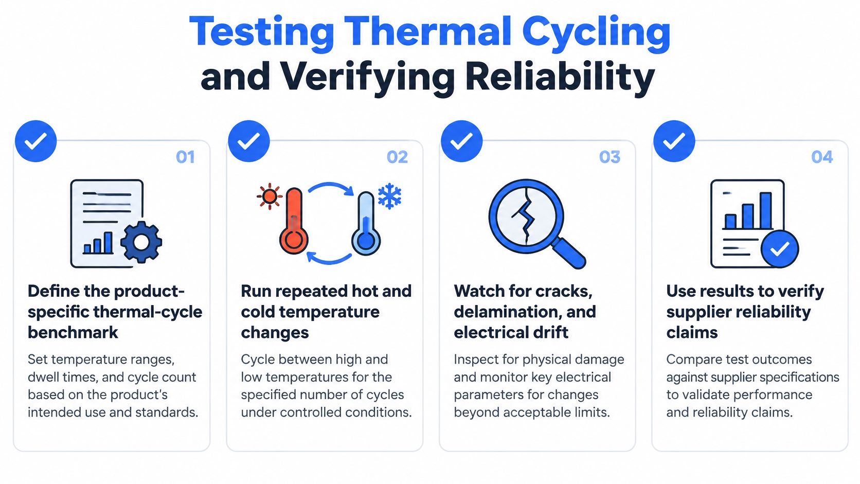
The checklist below turns a vague reliability claim into four questions you can audit.
<a id="what-published-results-actually-show"></a>
What Published Results Actually Show
In one published DBC study, standard substrates developed conchoidal fracture at copper layer edges after approximately 100 thermal shock cycles between -40°C and +150°C, whereas a reinforced design showed no delamination through 2,000 cycles under the stated method, as reported in a published study on advanced highly reliable DBC substrates. A separate power cycling evaluation found Al2O3 DBC stopped before 1,000 cycles because of excessive thermal resistance increase, while AlN and Si3N4 specimens completed more than 20,000 cycles without observable physical failure in that setup.
Don't copy those numbers into your specification. Thickness, copper pattern, solder interface, ramp rate, and temperature limits change the result. A bare substrate that survives a chamber can still fail after assembly because solder, a baseplate, fasteners, or an enclosure adds constraint.
More cycles aren't better evidence if the temperature profile and failure definition don't match field loading.
Write your own qualification plan:
- Define the specimen: Bare DBC, DPC, or AMB substrate, or a fully assembled module.
- Define the load: Temperature extremes, dwell, ramp or transfer conditions, and cycle count tied to your mission profile.
- Define failure: Cracking, delamination, insulation failure, or resistance drift, with limits set before testing starts.
- Define inspection: X-ray or scanning acoustic methods for hidden delamination, plus electrical and thermal resistance before and after cycling.
An EV inverter, an industrial converter, an LED module, and an RF package shouldn't automatically share one qualification. Ask your Ceramic PCB manufacturer for raw counts, sample size, and failure criteria, not a brochure phrase about high reliability.
<a id="evaluating-cost-lead-times-and-certifications"></a>
Evaluating Cost, Lead Times and Certifications
A ceramic PCB quote is a thermal decision dressed as a purchasing task. A premium substrate that doesn't lower device temperature in your assembly is just an expensive plate.
Heat leaves through a series path: silicon, die attach, copper, ceramic, interface material, heatsink, then air or liquid. That path works like several valves in line. Opening one valve does little if the next one is still closed, so judge AlN, Al2O3, DBC, DPC, thick film, AMB, or LTCC by the temperature drop they create inside your stack-up. Published package numbers can help, but only when power, die size, attach method, baseplate, mounting pressure, airflow, and failure metric resemble your build. Ask each Ceramic PCB manufacturer to show the assumed thermal path for your assembly, not only a datasheet conductivity value.
<a id="what-drives-price-and-lead-time"></a>
What Drives Price and Lead Time
- Substrate material and usable area: AlN, special grades, and poor panel utilization raise cost.
- Copper and geometry: Thick copper, tight isolation, and fine features increase process sensitivity.
- Complexity: Layers, cavities, holes, finishes, and singulation add steps and yield risk.
- Evidence scope: Dimensional reports, interface checks, electrical test, and thermal qualification take time.
- Volume and revisions: Prototypes carry setup cost, and late drawing changes can restart tooling.
Ask suppliers to separate non-recurring tooling from unit price and to quote prototype, pilot, and production quantities on the same revision. A lower unit bid can hide extra test coupons, rework, inspection time, or a narrower process window. Don't assume a universal cheapest to most expensive process order, because yield and inspection scope can reverse it.
Certifications need the same plain reading. Suppliers in this space often state ISO 9001, ISO 13485, IATF 16949, UL, and RoHS compliance. Those systems support quality management, medical or automotive discipline, safety recognition, and substance restrictions. They still leave open whether your ceramic grade, copper bond, termination, cleanliness limit, and thermal cycle profile fit the application. Treat certificates as entry requirements, then request stack-up records, lot traceability, inspection data, and paperwork that names the actual manufacturing site and product scope.
<a id="questions-to-ask-your-ceramic-pcb-supplier-and-next-steps"></a>
Questions to Ask Your Ceramic PCB Supplier and Next Steps
Bring a short, specific RFQ. Vague requests get vague quotes, and ceramic quotes built on guesses usually change later.
<a id="your-supplier-checklist"></a>
Your Supplier Checklist
- Substrates and processes: Which ceramic grades do you run, and do you offer DBC, DPC, thick film, AMB, or LTCC for this design?
- Finished geometry: What copper thickness, trace width, isolation gap, edge profile, and flatness can you hold on my artwork?
- Thermal evidence: How will you calculate or measure system level thermal resistance for my assembly?
- Qualification: What temperature profile, sample size, inspection method, and failure criteria will you use?
- Traceability: What material lot, process revision, and inspection records ship with the lot?
- Assembly path: Can prototypes move into low volume production without a drawing or process change?
Include ceramic type, ceramic and copper thickness, operating temperature, thermal cycle profile, surface finish, quantity ladder, and assembly needs in your RFQ. Attach the mission profile if reliability matters. A good Ceramic PCB manufacturer will push back on missing data instead of quoting around it.
For teams that want fabrication and assembly under one roof, turnkey PCB assembly services that combine sourcing and build can reduce hand off risk between bare substrate and finished module. Lianyuhong Technology Co.,Ltd offers ceramic fabrication on Al2O3 and AlN with DBC and thick film options, alongside turnkey SMT and THT assembly, DFM and BOM review on every order, and inspection and test options including SPI, AOI, X-ray, and functional test. Quick turn prototypes and global shipping through DHL, UPS, and FedEx support that path from first sample to low volume production.
Your next step is practical. Prepare your stack-up, thermal load, cycle profile, and quantity ladder, then request a written DFM and qualification review before you commit to material.
If you're ready to test whether alumina, AlN, DBC, or thick film fits your thermal design, send your drawings, copper requirements, and operating profile for a DFM, BOM, and stack-up review with quick turn ceramic prototyping and turnkey assembly options. Visit Lianyuhong Technology Co.,Ltd to request that review and get a quote based on your actual mission profile, not a generic cycle claim.