
Adding a bigger capacitor isn't a reliable way to remove high-frequency noise. Neither is scattering small capacitors around an IC and assuming the smallest value will handle the fastest edges. Both shortcuts ignore the current path through the component and the board.
On a schematic, a capacitor looks like a simple connection between power and ground. On the board, it behaves like capacitance, resistance, and inductance in series. Which element dominates changes with frequency, so a useful part in one band can become an obstacle in another.
Table of Contents
- Why a Real Capacitor Stops Filtering at High Frequency
- Self-Resonant Frequency by Capacitance Value
- How Package Size and Dielectric Shift the Curve
- Decoupling Ladders and Anti-Resonance Traps
- How to Choose and Place a High-Frequency Capacitor
- Confirm Your Capacitor Choice With Measurement
<a id="why-a-real-capacitor-stops-filtering-at-high-frequency"></a>
Why a Real Capacitor Stops Filtering at High Frequency
An ideal capacitor becomes easier for alternating current to pass through as frequency rises. Follow that model far enough, and the capacitor approaches a short circuit. That's the origin of the familiar advice to bypass high-frequency noise to ground.
A physical capacitor can't follow that ideal curve indefinitely. Current must travel through terminations, electrodes, and connections that resist rapid changes in current. At sufficiently high frequency, those connections matter more than the capacitance printed on the package.
<a id="start-with-a-tank-and-narrow-pipes"></a>
Start with a tank and narrow pipes
Think of a water tank connected through narrow inlet and outlet pipes. When flow changes slowly, water has time to enter and leave the tank, and the tank's storage capacity largely determines its response. When flow reverses rapidly, pipe resistance and the inertia of the moving water become important.
The illustration captures that shift from storage-dominated behavior to connection-dominated behavior.
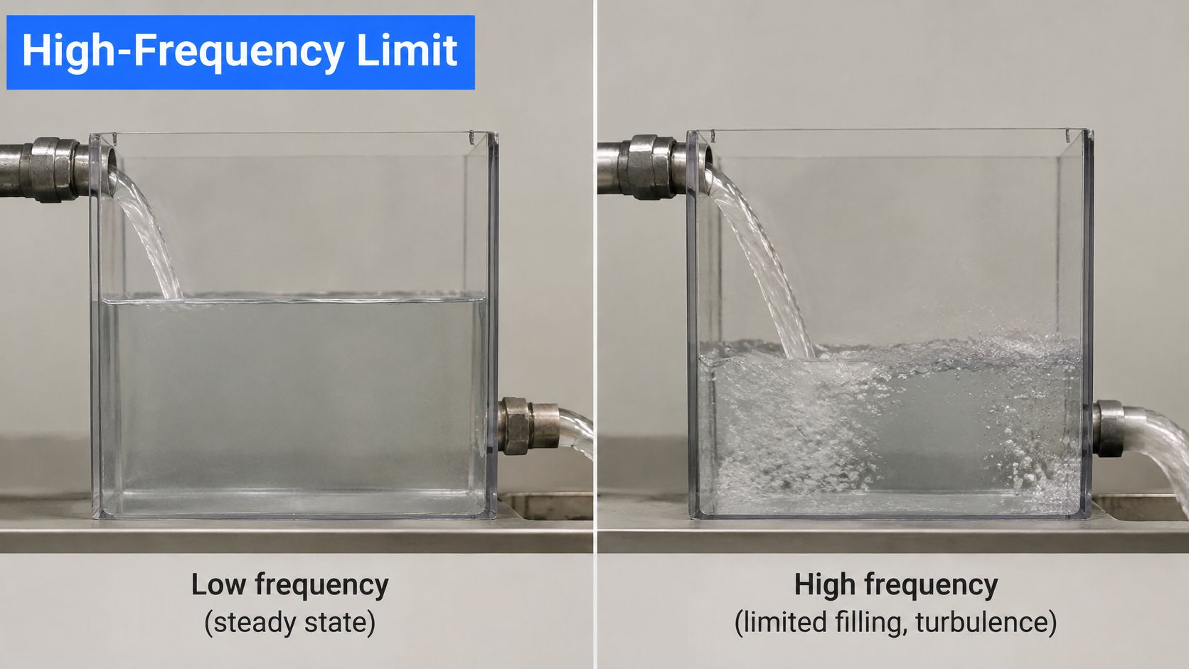
The electrical model has corresponding elements. Capacitance stores charge, equivalent series resistance, or ESR, dissipates energy, and equivalent series inductance, or ESL, opposes changes in current. These aren't separate components that someone forgot to draw; they're properties of the physical part.
ESR represents conductor losses in electrodes and terminations, along with an equivalent representation of dielectric losses. ESL comes from the magnetic field associated with the current path through the body and terminals. Once mounted, the pads, vias, traces, and return path add further inductance.
The water analogy has limits. A capacitor doesn't pass conduction current through its insulating dielectric, and a real component's losses change with frequency. Still, the analogy helps explain why unlimited storage capacity can't compensate for a restrictive connection.
<a id="sketch-the-impedance-before-choosing-the-part"></a>
Sketch the impedance before choosing the part
Draw frequency along the horizontal axis and impedance magnitude vertically, using logarithmic scales. A simple series model produces a broad V-shaped curve with a rounded bottom. The left arm slopes downward, the right arm slopes upward, and resistance sets the floor.
| Region of the curve | Dominant behavior | What it means on the board | |---|---|---| | Descending left arm | Capacitive reactance | More capacitance can reduce impedance | | Rounded minimum | Resistive loss near resonance | ESR limits the lowest available impedance | | Rising right arm | Inductive reactance | Reducing connection inductance becomes more useful than adding capacitance |
At self-resonance, capacitive and inductive reactance cancel. In the simple model, the remaining impedance is ESR. That's why the lowest point isn't a perfect short.
A low-ESR capacitor produces a deep, relatively sharp minimum. More resistance produces a higher floor and a less pronounced resonance. Don't confuse that flatter curve with better filtering: damping can suppress ringing, but the higher impedance may exceed the rail's noise budget.
Dielectric loss also contributes damping. Manufacturers often describe it through the dissipation factor, which relates dielectric loss to reactive behavior under specified test conditions. It deserves particular attention with Class 2 ceramics and with film capacitors used in resonant circuits, where circulating current can cause heating.
A capacitor doesn't become useless when it becomes inductive. It becomes unsuitable when its installed impedance is too high for the job.
That distinction matters. A part can remain a helpful shunt slightly above self-resonance if its impedance is still sufficiently low. Conversely, a part operating below resonance can already be inadequate because its capacitive reactance is too high.
<a id="read-the-plot-as-a-circuit-model"></a>
Read the plot as a circuit model
Start by locating the impedance minimum on the manufacturer's plot. Then examine how quickly impedance rises on the high-frequency side and how pronounced the minimum looks. Those features tell you about resonance, inductance, and damping.
Check what the plot really represents. A typical component curve may describe a particular measurement fixture without reproducing your mounting geometry, operating bias, or temperature. If the manufacturer supplies ESR curves or simulation models, use them to distinguish resistive loss from total impedance.
For capacitor high frequency behavior, the useful question isn't whether the capacitance is large enough. It's whether the complete branch provides sufficiently low impedance over the required band. A decoupling capacitor is a band-limited impedance-control element, not a universal high-frequency short.
<a id="self-resonant-frequency-by-capacitance-value"></a>
Self-Resonant Frequency by Capacitance Value
The ranges below reflect typical small-package surface-mount ceramics, such as 0402 parts, mounted with short, low-inductance connections. Use them to screen candidates, then confirm against the exact part's impedance curve.
| Capacitance | Typical self-resonant frequency | Behavior above that frequency | |---|---|---| | 10 pF | Roughly 1 to 3 GHz | Inductive, although a low-inductance mounting may retain useful shunting | | 100 pF | Roughly 300 MHz to 1 GHz | Impedance rises as inductive reactance becomes dominant | | 1 nF | Roughly 100 to 300 MHz | Evaluate the rising impedance against the rail requirement | | 10 nF | Roughly 30 to 80 MHz | No longer behaves as an ideal capacitive bypass | | 1 µF | Roughly 3 to 10 MHz | May still contribute if its branch impedance remains low enough | | 10 µF | Roughly 1 to 3 MHz | Usually serves storage and slower transient support rather than the fastest local demand |
These are screening ranges rather than guaranteed assignments. Different internal constructions, dielectrics, and mounting arrangements can move a given part well outside the band shown.
<a id="why-larger-capacitance-usually-moves-resonance-lower"></a>
Why larger capacitance usually moves resonance lower
Resonance occurs where inductive and capacitive reactance balance, following f = 1/(2π√(LC)). With inductance held constant, frequency scales with the inverse square root of capacitance. Each tenfold increase in capacitance therefore lowers resonance by a factor of about three in the same package.
Effective capacitance matters more than nominal capacitance. A ceramic capacitor under DC bias can hold far less than its labeled value, which pushes its actual resonance higher than the unbiased figure. Installation shifts the curve again by adding series inductance through pads, traces, and vias.
Consider a designer comparing a small RF capacitor against a much larger decoupling part. The larger capacitor wins at low frequencies, where its impedance sits well below the smaller part's. The smaller part keeps falling past the point where the large one has already turned inductive. The right choice changes with the frequency band under examination.
<a id="use-the-table-as-a-screening-method"></a>
Use the table as a screening method
Find the intended capacitance, obtain the exact manufacturer part number, and locate its impedance valley. Compare the complete curve with the noise spectrum you need to control, rather than comparing only the self-resonant frequency with the clock frequency.
- Check the operating conditions: Confirm that the model represents the relevant bias and temperature.
- Include the mounting path: Add the connection inductance before accepting the predicted response.
- Compare impedance, not labels: Reject a branch that exceeds the required impedance where the load needs support.
A noise component above self-resonance warns you to inspect the inductive side of the curve. The practical pass or fail is whether the mounted capacitor network meets the required impedance at that frequency.
<a id="how-package-size-and-dielectric-shift-the-curve"></a>
How Package Size and Dielectric Shift the Curve
| Package | Practical effect | |---|---| | 0201 | Short body can support low component inductance; demanding to hand-place and inspect | | 0402 | Common high-frequency decoupling choice with a useful balance of size and assembly practicality | | 0603 | Often accommodates greater capacitance or voltage capability, but its longer current path can increase component inductance |
Package codes identify physical formats, not guaranteed electrical performance. Don't attach a universal ESL value to a package or assume a fixed improvement when moving between sizes. Internal electrode geometry, terminal arrangement, and mounting all affect the result.
<a id="shorten-the-current-path-without-losing-needed-capacitance"></a>
Shorten the current path without losing needed capacitance
For otherwise comparable conventional parts, a shorter body generally helps reduce component inductance. However, the board connection can outweigh that improvement. A compact capacitor connected through a long trace and a remote ground via may perform worse than a larger part with a tightly coupled return.
Say a designer replaces a 0603 capacitor with a 0402 part but leaves the original widely spaced vias in place. The component may improve while the installed branch barely changes. Moving the vias and shortening the pad connections can matter more than the package substitution.
Assembly also constrains the choice. A package that's awkward to rework or inspect may create unnecessary development risk, particularly on prototypes that will undergo repeated component changes.
Practical rule: Choose the smallest manufacturable package that supplies the required effective capacitance and voltage capability, then evaluate its actual mounting loop.
<a id="choose-the-dielectric-for-the-electrical-job"></a>
Choose the dielectric for the electrical job
C0G, also called NP0, offers stable capacitance with temperature and applied voltage, along with low dielectric loss. It suits RF matching, timing, and resonant circuits where the capacitance itself defines circuit behavior. Its limitation is that substantial capacitance requires more volume.
X7R and X5R ceramics provide much more capacitance in a compact body. Their effective capacitance changes with DC bias, temperature, and aging, so the value printed in the part description isn't necessarily the value available during operation.
For an RF matching network, a C0G part helps keep tuning predictable and limits dielectric loss. For a digital supply rail, an X7R part can provide useful local charge storage, provided its bias curve leaves enough capacitance at the working voltage.
Temperature behavior shouldn't be simplified to a guaranteed reduction in value. Capacitance can move within the dielectric's characteristic range, while DC bias commonly reduces effective capacitance in Class 2 ceramics. Use the selected part's curves rather than treating the dielectric designation as a complete model.
<a id="decoupling-ladders-and-anti-resonance-traps"></a>
Decoupling Ladders and Anti-Resonance Traps
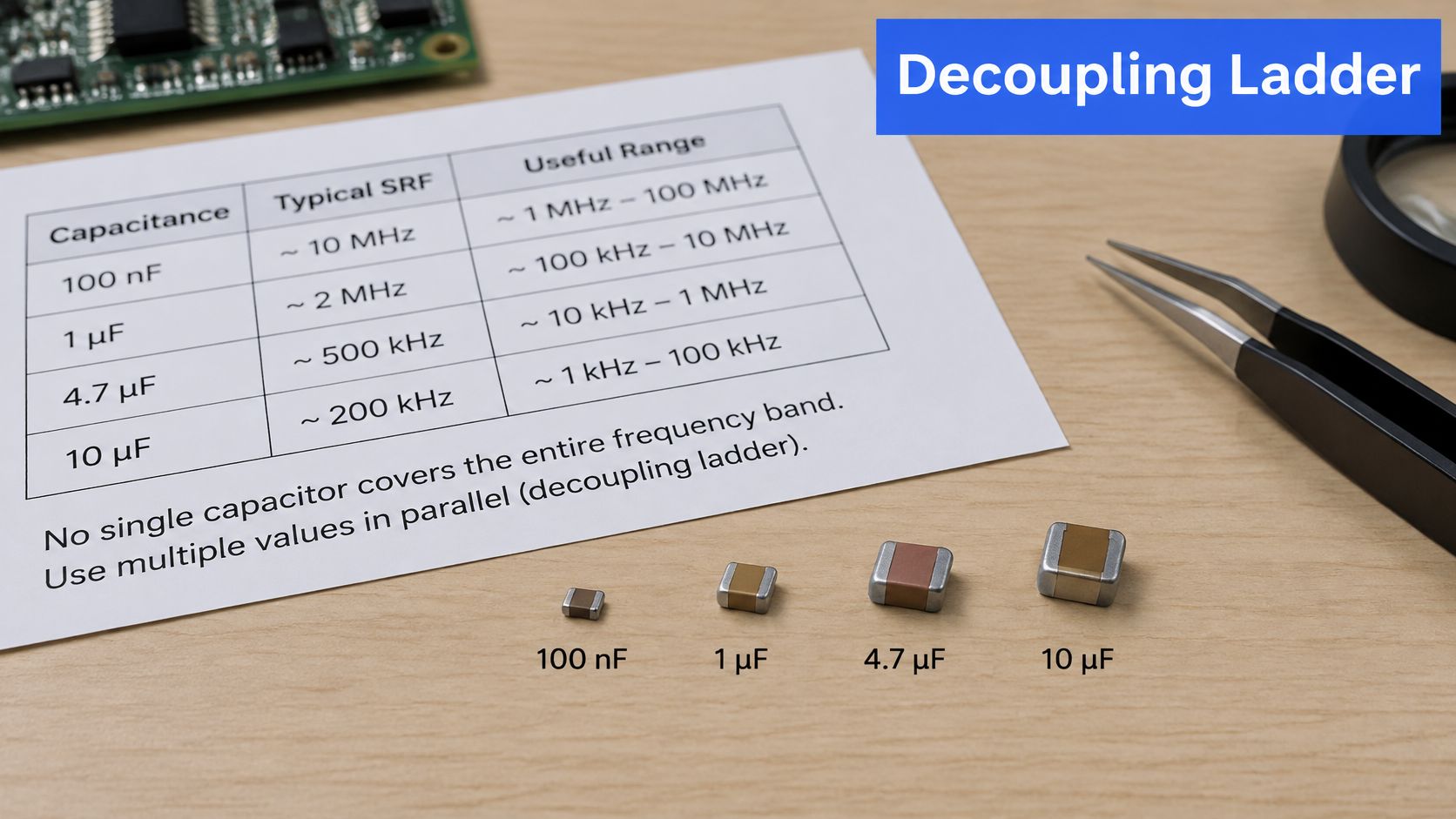
| Value | Typical package | Covers roughly | Role on the rail | |---|---|---|---| | 10 µF | Choose for effective storage and voltage capability | Slower load variations | Supplies charge while upstream delivery responds | | 1 µF | 0603 as an illustrative starting choice | Intermediate transient demand | Supports the region between bulk storage and local bypassing | | 100 nF | 0402 as an illustrative starting choice | Local switching demand within its low-impedance region | Supports current changes near the IC | | 10 nF | 0402 as an illustrative starting choice | A higher-frequency window if the installed curve supports it | Supplements local decoupling where analysis shows a gap | | 100 pF | 0402 C0G as an illustrative starting choice | A narrow RF-oriented window | Addresses a demonstrated high-frequency requirement |
This is an example of possible roles, not a required shopping list. The values don't define fixed frequency bands, and populating every row doesn't guarantee broadband coverage. Some rails work better with repeated values and controlled damping than with a descending sequence of capacitances.
The ladder concept is easiest to visualize as overlapping regions of useful impedance.
<a id="parallel-capacitors-can-create-an-impedance-peak"></a>
Parallel capacitors can create an impedance peak
Between the resonances of different capacitor branches, one branch may appear inductive while another remains capacitive. Their admittances can partially cancel, producing anti-resonance. Interconnect inductance can make the peak worse, but a long connection isn't required for the effect to occur.
The combined impedance plot then shows a spike between valleys. Adding a capacitor can therefore increase impedance over part of the spectrum, even though it reduces impedance elsewhere. That's the intuition failure behind many unsuccessful attempts to fix ringing by adding more ceramics.
The height of the peak depends on losses as well as reactive values. Very low ESR can make an otherwise attractive capacitor combination sharply resonant.
<a id="correct-the-network-rather-than-adding-parts-blindly"></a>
Correct the network rather than adding parts blindly
Try changes in a controlled sequence and compare the resulting curves.
- Change a value or remove a redundant branch: Shift the interaction away from the sensitive band without opening another gap.
- Introduce deliberate damping: A resistor in a selected capacitor branch or a suitable lossy capacitor can reduce the peak. Check pulse current and dissipation.
- Use ferrites only with a complete model: A bead can provide useful loss, but its reactive behavior and bias dependence can introduce another resonance.
- Reduce connection inductance: Improve the local placement and return geometry instead of treating the schematic as the complete circuit.
These choices belong alongside the return-path and stack-up decisions described in high-speed PCB design. Evaluate the impedance at the load, not just at the capacitor bank.
A ladder is only as useful as its worst in-band peak. Broad low impedance matters more than an impressive collection of deep, isolated minima.
<a id="how-to-choose-and-place-a-high-frequency-capacitor"></a>
How to Choose and Place a High-Frequency Capacitor
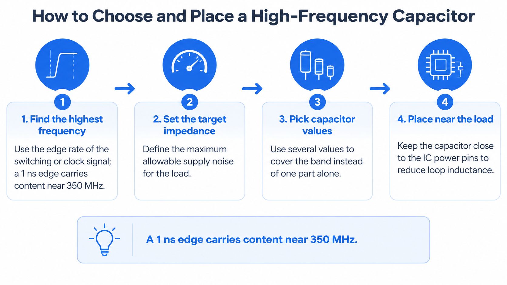
Selection works best when you turn the noise requirement into an electrical limit before opening a component catalog. The process graphic summarizes that workflow; use the actual signal waveform and component models rather than treating its illustrative edge-rate estimate as a universal cutoff.
<a id="turn-the-requirement-into-a-component-shortlist"></a>
Turn the requirement into a component shortlist
-
Identify the relevant frequency content. Use switching edge rates, load-current behavior, and sensitive RF bands. Don't use clock repetition rate alone: a slowly repeating signal can still have fast edges, and an edge-rate bandwidth estimate isn't a hard spectral boundary.
-
Set the target impedance. Use (Z_{\text{target}}=\Delta V/\Delta I), where the voltage term is the allowable disturbance and the current term is the relevant load step. Treat this as an engineering starting point, not proof that a complicated load has a flat requirement across every frequency.
-
Select candidate values from actual impedance curves. Look for coverage of the required band without excessive peaks. The common slip is choosing familiar nominal values first and trying to justify them afterward.
-
Check package, voltage capability, and effective capacitance together. Apply the manufacturer's DC-bias and temperature information before accepting the available charge storage. A higher voltage rating alone doesn't guarantee favorable bias behavior.
<a id="make-the-installed-circuit-match-the-model"></a>
Make the installed circuit match the model
-
Assign the dielectric to the function. Use stable, low-loss material where tuning and resonant behavior matter; use high-capacitance ceramics where storage density is more important. Don't replace an RF tuning capacitor with a Class 2 part merely because its nominal value matches.
-
Inspect losses and resonance under relevant conditions. Review impedance, ESR, and available simulation models, including temperature dependence. Avoid treating a room-temperature typical curve as a guaranteed worst-case boundary.
-
Place the capacitor around the actual current loop. Connect the load, capacitor, and return with a compact geometry over a continuous reference. Physical closeness is misleading if routing forces the current through a detour.
-
Design the pad-to-plane connections deliberately. Put a dedicated via adjacent to each pad where the stack-up permits, or use an appropriate via-in-pad structure. Additional vias may help, but long necks, distant returns, and unnecessary shared connections can undermine the benefit.
A high-frequency PCB stack-up and fabrication plan should support the intended return geometry and assembly method. Material selection can't compensate for an unnecessarily inductive capacitor connection.
Don't approve a placement because the capacitor looks close to the IC. Trace the complete outgoing and return-current paths.
<a id="pre-release-checklist"></a>
Pre-release checklist
- Spectrum defined: Relevant edge behavior and sensitive bands are identified.
- Impedance budget set: Allowed voltage disturbance and load-current demand are documented.
- Values modeled: The combined network has no unacceptable in-band peak.
- Derating checked: Effective capacitance and voltage capability are adequate.
- Dielectric matched: Stability and loss suit the circuit function.
- Curves reviewed: Component models reflect the relevant operating conditions.
- Loop inspected: The load-to-capacitor path and return are compact.
- Vias verified: Pad connections reach the intended planes without avoidable detours.
<a id="confirm-your-capacitor-choice-with-measurement"></a>
Confirm Your Capacitor Choice With Measurement
A datasheet curve describes a component under defined conditions. Your load sees a mounted network that includes planes, vias, package connections, and the regulator. Approval should depend on that network, not the component curve alone.
<a id="measure-impedance-and-transient-behavior"></a>
Measure impedance and transient behavior
Measure rail impedance with an impedance analyzer or a vector network analyzer using a suitable calibrated fixture. For low-impedance rails, a shunt-through arrangement may be appropriate; account for fixture effects, instrument limits, DC isolation, and safe connection to an energized rail. Keep connections compact and measure at the load location.
Then inspect rail noise with an oscilloscope during representative load activity. Use a ground spring or a suitable low-inductance power-rail probe connection rather than a long ground clip. Otherwise, probe-loop pickup can resemble genuine rail ringing.
- Compare the frequency-domain result: Check every relevant valley and peak against the target, without assuming a valley must occur between particular ladder values.
- Compare the time-domain result: Confirm that droop, overshoot, and ringing stay within the load's requirements.
- Repeat at operating conditions: Exercise the relevant bias, temperature, and load states.
Keep power-rail impedance distinct from transmission-line impedance when planning PCB impedance control. Both require disciplined geometry, but they answer different electrical questions.
Measure the rail, compare it with the target impedance, and commit only when the measured curve passes at the frequencies that matter.
Lianyuhong Technology Co.,Ltd offers high-frequency PCBs using Rogers, PTFE, and high-speed materials for RF and microwave applications, with low-Dk/Df material options and SET2DIL, Delta-L, and VNA testing. To connect your capacitor models with a manufacturable stack-up and compact return paths, visit Lianyuhong Technology Co.,Ltd to discuss PCB fabrication, layout, and assembly requirements.