
“Keep traces short, match the pairs, and control impedance” is useful advice, but it isn't a high-speed qualification plan. A board can pass its impedance coupon and still lose enough signal energy to fail at the receiver. Short routes won't rescue an inaccurate material model, an unbudgeted connector, or a fabrication substitution.
High speed PCB design starts with a signed electrical and manufacturing package, not routing. Every important simulation assumption needs a corresponding drawing note and an acceptance check. Otherwise, you're approving a model without defining how anyone will build or verify it.
Table of Contents
- Freeze the Impedance Brief Before Routing
- How to Sequence a High-Speed Layout
- Length Matching and Skew for Differential Pairs
- Return Paths and Via Stubs That Close the Eye
- Fabrication Specs That Keep Simulation Honest
- Signal Integrity Checks on a Startup Budget
<a id="freeze-the-impedance-brief-before-routing"></a>
Freeze the Impedance Brief Before Routing
Start with a target table that the electrical engineer, layout engineer, fabricator, and test owner can sign. Record the interface requirements first, then distinguish requirements from convenient starting points.
The IPC-2141 controlled-impedance overview describes the approximate transmission-line trigger of one-sixth of the relevant signal wavelength, typical targets of 50 ohms single-ended and 90–100 ohms differential, and an ordinary production tolerance around ±10 percent. These are starting rules, not permission to override an interface specification.
High-speed targets to freeze before routing
| Decision | Working target | What changes it | |---|---|---| | Transmission-line trigger | Electrical length beyond about one-sixth of the edge wavelength | Rise and fall time, not the clock frequency | | Single-ended impedance | About 50 ohms | The interface specification overrides the rule of thumb | | Differential impedance | About 90–100 ohms | Follow the serial-link specification, not a default pair | | Production tolerance | About ±10 percent | Tighten when the channel budget requires it and fabrication can support it | | Adjacent pair spacing | Reserve generous separation wherever the floorplan allows | Dense BGA escape requires a crosstalk check | | Reference | Continuous plane under the entire route | A split, void, or layer change requires a defined return-path transition |
Use the fastest applicable transmitter edges when establishing electrical length. A slowly toggling control net can still need transmission-line treatment if its driver switches sharply. Don't classify nets from the clock label alone.
<a id="freeze-the-release-package"></a>
Freeze the release package
Before routing a critical net, approve these items:
- Interface impedance and edge rate. Include the operating mode, transmitter model, receiver requirements, and allowable channel loss. Record which specification revision governs the decision.
- Solved routing geometry. Save field-solver width and spacing against the actual dielectric construction and finished copper thickness. A geometry value without its stack-up isn't a reusable impedance rule.
- Reference-layer assignment. Identify the reference plane for every permitted signal layer. Mark prohibited routing regions around voids, cutouts, and connector clearances.
- Via construction. Choose the transition structure and define residual-stub control. If back-drilling is required, specify the target layer, drilling direction, depth tolerance, and protected connection.
- Acceptance ownership. Name who approves impedance measurements, who approves insertion loss, and what evidence each person needs before release.
Width and spacing don't establish impedance by themselves. Dielectric thickness, dielectric constant, copper thickness, and reference geometry all contribute. Etching and lamination tolerances must therefore be represented in the approved construction, not treated as manufacturing details someone can settle later.
Release rule: A clean schematic proves connectivity. It doesn't prove that the channel you've simulated can be manufactured.
The historical pressure is clear: the PCI-SIG specification webinar traces PCIe from 2.5 GT/s in 2003 to 32.0 GT/s in 2019. At those faster transfer rates, treating packages, connectors, and board transitions as incidental geometry becomes increasingly difficult to justify.
Use an impedance-control PCB checklist to document the construction and acceptance method, rather than attaching only an impedance label to the net class. A generic FR-4 quotation doesn't preserve the assumptions behind a low-loss model, copper-profile requirement, or back-drill instruction. Get those assumptions into the release package before placement makes them expensive to change.
<a id="how-to-sequence-a-high-speed-layout"></a>
How to Sequence a High-Speed Layout
-
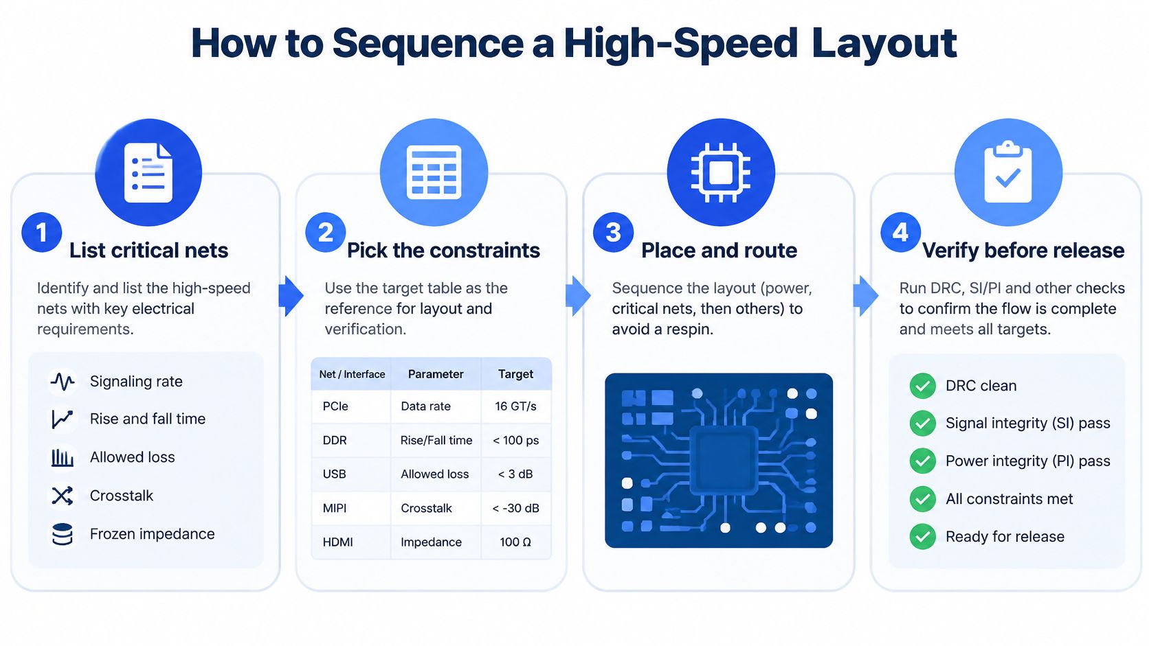
List every critical interconnect before placement. Record signaling rate, rise and fall time, impedance, allowable loss, crosstalk, and timing constraints. Include clocks and fast control signals, not just interfaces that carry a high-speed marketing label. Give each constraint an owner so unresolved requirements don't become CAD defaults.
-
Choose the stack-up around the channels. Put critical routing layers beside continuous reference planes and reserve routing capacity before filling the board with less sensitive nets. Stripline can provide a more shielded routing environment, but its dielectric exposure and via access still need evaluation. Request frequency-dependent Dk and Df for the proposed construction, rather than accepting a single datasheet value.
-
Solve the manufacturable geometry. Use a field solver with the proposed finished copper, dielectric height, and pair spacing. Check whether the resulting dimensions can escape the package without long neck-downs. If they can't, revise placement, stack-up, or escape technology before committing to the route.
-
Place components to protect the channel budget. Orient connectors and devices so critical pairs don't weave around unrelated circuitry. Reserve space for return vias, termination components, and test structures. A shorter route isn't automatically better if achieving it requires awkward transitions or a compromised reference.
The NASA High-Speed PCB Design Guide recommends minimizing discontinuities with smaller microvias or HDI structures and keeping neighboring differential pairs at least five trace widths apart where practical. Apply that separation deliberately in the constraint manager, and use coupling analysis where the escape region can't accommodate it.
The sequence should remain visible during layout reviews.
<a id="finish-with-a-channel-review"></a>
Finish with a channel review
-
Route critical pairs with stable geometry. Stay on the assigned layer where practical and avoid reference-plane splits. Confine unavoidable neck-downs to modeled escape or connector regions. Don't let an autorouter introduce repeated width changes merely because every individual segment passes clearance rules.
-
Model the complete signal path. Combine package, board routing, vias, connector, and termination in the channel model. Check model reference planes and port definitions before connecting S-parameter blocks. Otherwise, you can accidentally omit a launch or count the same structure twice and obtain a convincing but misleading result.
-
Run SI, PI, and DFM reviews before fabrication. Evaluate channel behavior alongside power-distribution noise and manufacturing limits. Review the exported fabrication data, not only the live CAD database, and define the coupon correlation plan before releasing the files.
Material selection belongs in this sequence, not in purchasing cleanup. The high-frequency PCB capability overview provides useful context for evaluating laminate and measurement requirements against the intended construction.
The expensive mistake is routing first and correcting impedance afterward. By then, placement may have fixed the wrong layer count, escape geometry, and plane arrangement. The pre-fabrication handoff should contain approved layer assignments, reference planes, pair clearances, channel models, and a disposition for every exception.
<a id="length-matching-and-skew-for-differential-pairs"></a>
Length Matching and Skew for Differential Pairs
-
Set a delay budget before adding length. Take intra-pair skew and lane-to-lane timing requirements from the interface specification. These aren't interchangeable constraints. Some links care strongly about balance within a pair but allow the receiver to accommodate differences between lanes.
-
Route for symmetry before tuning. Keep both traces on the same layer with consistent geometry through ordinary routing regions. Match the escape topology and avoid sending one member around an obstacle while the other takes a direct path. It's easier to preserve balance than to repair an asymmetric route with extra copper.
-
Correct mismatch near its source. Where the interface guidance permits it, compensate close to the pin or escape region that introduced the mismatch. Avoid inserting dense tuning into an otherwise uniform coupled run. The compensation itself changes coupling and must be evaluated, not accepted because the length counter turns green.
-
Give tuning patterns room. Separate neighboring meander legs, keep them away from unrelated aggressors, and avoid crowding them against vias or connector launches. Closely packed serpentine routing can produce a different delay from the simple added-length estimate.
-
Include vertical and component paths. Compare via structures, connector pin paths, and available package delay information. Matched surface copper doesn't establish matched end-to-end delay when the pair members encounter different transitions.
<a id="prove-delay-rather-than-matching-artwork"></a>
Prove delay rather than matching artwork
Use electrical delay as the review quantity wherever the tools and models support it. CAD length is a useful control, but it can't fully describe different propagation environments or asymmetric discontinuities.
A representative coupon can support time-domain delay measurements and reveal whether the manufactured geometry behaves as expected. Receiver eye width then shows whether residual skew leaves adequate timing margin in the complete channel.
Equal CAD lengths are a routing result. Acceptable end-to-end skew is the engineering requirement.
Don't add tuning solely to make a report look tidy. If a route already meets its timing budget, unnecessary meanders consume space and introduce coupling. Review connector pin-to-pin differences and transition symmetry before spending that space on trace-length correction.
<a id="return-paths-and-via-stubs-that-close-the-eye"></a>
Return Paths and Via Stubs That Close the Eye
An unused via barrel isn't merely extra copper. It's an open transmission-line branch, and the peer-reviewed via model hosted by Missouri S&T explains why a stub approaching a quarter wavelength can create a strong resonant discontinuity. The practical question is whether that resonance and its surrounding degradation intersect the channel's useful spectrum.
Physical inspection helps verify that the intended transition was manufactured.

Estimate electrical stub length using the actual stack-up propagation characteristics and the significant spectral content of the transmitter edge. Don't judge the risk from the interface's fundamental frequency alone. A channel can pass continuity testing while suffering excess loss, deterministic jitter, or intermittent receiver errors.
<a id="choose-the-transition-in-the-right-order"></a>
Choose the transition in the right order
- Assign the routing layer first. The destination layer determines how much unused barrel remains. Choosing a generic through-via before layer assignment hides the problem.
- Evaluate blind, buried, or laser-microvia options. These can avoid unused barrel, but they introduce fabrication, reliability, and cost considerations. Use the simplest qualified structure that satisfies the channel.
- Specify back-drilling when needed. State the allowable residual stub and drilling tolerance, not just a request to back-drill. The process must remove enough barrel without damaging the intended connection.
- Provide a nearby return transition. Ground-return vias must connect the relevant reference planes without landing in clearance voids.
- Simulate the full via field. Include pads, antipads, barrels, residual stubs, return vias, and neighboring connector or package structures.
A nominal simulation isn't enough when drill depth and dielectric thickness affect the outcome. Run the plausible manufacturing extremes, including the longer residual stub and the geometry combinations that worsen transition mismatch.
The video provides another view of the design considerations around high-speed interconnects.
<iframe width="100%" style="aspect-ratio: 16 / 9;" src="https://www.youtube.com/embed/icRzEZF3eZo" frameborder="0" allow="autoplay; encrypted-media" allowfullscreen></iframe><a id="match-the-evidence-to-the-failure"></a>
Match the evidence to the failure
Use TDR to locate a transition-related impedance disturbance, then use insertion-loss measurement to determine whether a damaging notch falls in the operating band. A microsection, when required by the quality class or inspection plan, checks physical construction and residual barrel.
Don't prescribe the expected TDR shape so narrowly that a different defect gets dismissed. Pads, antipads, launches, and stubs interact, so compare the measured signature with the modeled structure.
A finished-hole diameter alone doesn't define a high-speed via. The acceptance package also needs depth control, reference continuity, and the measured channel response. Those are the details that distinguish a manufacturable hole from an acceptable transition.
<a id="fabrication-specs-that-keep-simulation-honest"></a>
Fabrication Specs That Keep Simulation Honest
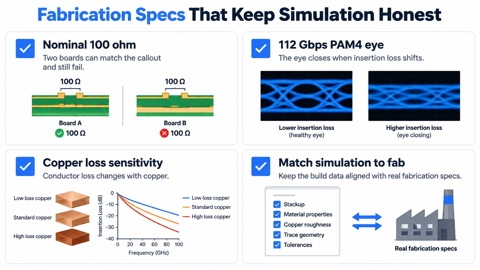
Impedance-controlled isn't the same as high-speed-qualified. Boards can meet the same nominal impedance while differing materially in insertion loss. A TDR pass doesn't validate the conductor-loss or dielectric-loss assumptions used in the channel simulation.
The AtlasPCB analysis of signal integrity and metallization describes copper-roughness sensitivity at 112-Gbps PAM4 and notes drawing requirements such as signal-layer Rz limits near 2.0 micrometers. That's an example of a construction-specific requirement, not a universal roughness limit for every high-speed board.
The drawing must preserve the assumptions that matter to the channel.
<a id="turn-model-inputs-into-acceptance-requirements"></a>
Turn model inputs into acceptance requirements
Simulation assumptions and what to accept on the board
| Model assumption | Request on the drawing | Acceptance check | |---|---|---| | Dielectric constant and loss | Dk and Df versus frequency for the proposed construction | Solver inputs cover the band established from the transmitter edge | | Copper roughness | Measurement method and layer-specific Rz requirements | Huray or Hammerstad–Jensen model parameters correspond to the specified copper profile | | Trace geometry | Finished width and spacing after etch | Field solver updated to measured representative geometry | | Glass and resin | Glass style, resin content, and substitution controls | Construction records and measured loss remain within approved limits | | Impedance | Coupon built on the routing stack-up | TDR meets the signed interface-specific tolerance | | Channel loss | Insertion-loss limit and defined measurement method | Measured loss correlates with the sign-off model within agreed uncertainty |
A roughness number without a measurement method is incomplete. Don't assume a reported surface metric maps directly to every roughness-model parameter. Establish which copper surface the measurement represents and how the model translates that information into conductor loss.
Finished geometry matters for the same reason. The CAD width isn't necessarily the manufactured conductor cross-section, and plating can change the structure beyond the nominal base-copper description. Use representative measured geometry when investigating a simulation-to-test mismatch.
<a id="control-substitutions-and-repeat-builds"></a>
Control substitutions and repeat builds
Resin content, glass construction, copper treatment, plating, and registration can change channel behavior even when purchasing continues to use the same stack-up name. Put approval requirements around changes that affect the electrical model. A procurement substitution shouldn't become an undocumented SI experiment.
Use PCB design standards to organize drawing requirements and inspection references, but keep interface-specific acceptance criteria explicit. A general workmanship requirement doesn't replace a channel-loss limit.
Procurement check: If the quotation doesn't identify the electrically important construction, purchasing hasn't secured the construction the simulation approved.
We offer low-loss Rogers and PTFE constructions, HDI with laser microvias and back-drill technology, and VNA or SET2DIL measurement, alongside schematic capture, layout, SI/PI simulation, and DFM review. Send the stack-up and critical-net list for engineering review before routing locks the rest of the board around them.
Don't release a repeat build until coupon TDR and measured insertion loss correlate with the approved model. Define the allowable correlation error in advance, and investigate discrepancies rather than adjusting model inputs solely to produce a match. Keep the accepted construction, model version, coupon results, and manufacturing revision together.
<a id="signal-integrity-checks-on-a-startup-budget"></a>
Signal Integrity Checks on a Startup Budget
Spend the measurement budget on decisions, not instrument names. The signal-integrity review available through SSRN identifies reflections, crosstalk, jitter, ground bounce, modeling, and TDR/VNA correlation as central workflow elements. For a small team, the useful approach is to assign each measurement a release question.
<a id="prototype-gate"></a>
Prototype gate
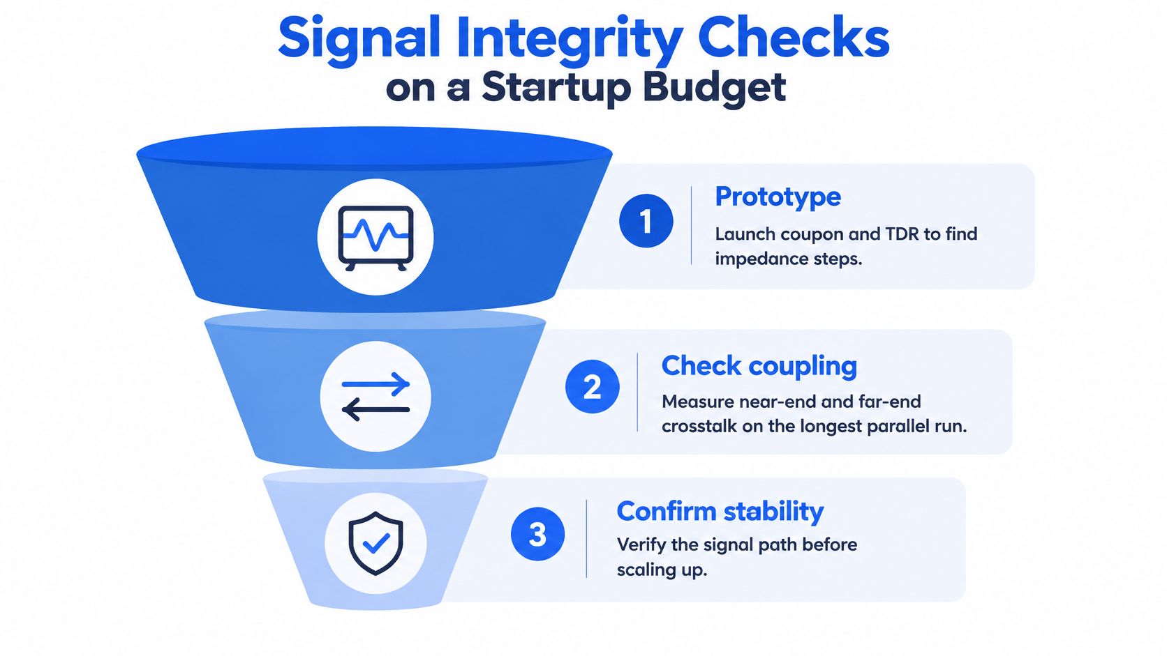
Start with a launch coupon and TDR when the main uncertainty is a discontinuity. Compare measured and simulated signatures before assuming that every unexpected feature belongs to the PCB routing rather than the fixture.
Measure near-end and far-end crosstalk on the longest relevant parallel region when coupling is a credible risk. A full VNA campaign can wait if those early checks isolate the dominant uncertainties and the loss budget isn't already marginal.
Use staged checks to keep the investigation focused.
What each signal-integrity check is worth
| Check | It can prove | It cannot prove | Use it at | |---|---|---|---| | TDR on a coupon | Localized impedance steps and stub-related disturbances | Insertion loss or bit-error rate by itself | Every prototype | | NEXT and FEXT | Coupling on the tested parallel run | A resonant via notch | Prototype, if pairs run side by side | | VNA S-parameters | Return loss and insertion loss versus frequency | System BER by itself | Pre-production, or sooner if the loss budget is tight | | Eye diagram | ISI and jitter under the tested settings, plus evidence for equalization needs | Margin across lots and temperature | After the channel is stable | | BER | Errors under the stress actually applied | Which discontinuity caused them | Production qualification gate |
<a id="pre-production-and-production-gates"></a>
Pre-production and production gates
At pre-production, measure insertion and return loss using a representative coupon or a fixture whose contribution can be removed reliably. De-embed when launches and fixtures would otherwise obscure the board behavior you're trying to accept. Check that de-embedding remains credible over the band of interest.
Keep package loss separate from board loss when diagnosing a discrepancy, then combine the validated models for system prediction. Use measured S-parameters in the channel simulation to evaluate eye behavior and estimate BER with the actual transmitter, receiver, and equalization assumptions.
Test the voltage and temperature conditions the team can support, and document the conditions it couldn't cover. An open eye at a comfortable bench setting isn't evidence of adequate margin across connector variation, assembly tolerance, and manufacturing lots.
At production, sample representative coupons by lot under a defined control plan. Requalification should follow electrically significant process changes, not merely a new CAD revision.
Write concrete pass rules into the review:
- Impedance passes the agreed tolerance using the approved measurement setup.
- Loss passes the channel limit, without a resonant notch in the operating band.
- Coupling passes the applicable interface budget under representative aggressor activity.
- Receiver performance passes the eye-mask and BER requirements under documented stress conditions.
- Uncertainty is accounted for through calibration, fixture removal, repeatability, and available environmental coverage.
Rent equipment or purchase targeted laboratory time when it resolves a specific release risk. Don't skip necessary evidence, but don't pay for a broad measurement campaign before you've established what result would change the design.
We provide schematic capture, PCB layout, SI/PI simulation, DFM review, and fabrication options for controlled-impedance, low-loss, and HDI channels. Visit Lianyuhong Technology Co.,Ltd with your proposed stack-up, critical-net list, and channel requirements so we can review the construction and acceptance checks before critical routing begins.