
The thermal camera finds it before the bench does. A 30 W LED engine, a half-bridge module, or an RF amplifier on FR-4, and the spot under the die is running far hotter than the case you modeled. You add thermal vias, then a thicker heat sink, then a fan. The hotspot shifts. It doesn't shrink.
Ceramic substrates are the next move, and they're a different category of board. A ceramic PCB material replaces the epoxy-glass laminate with a rigid, non-porous insulating plate, usually alumina or aluminum nitride, bonded to copper. Heat leaves through the plate instead of spreading sideways into more laminate, and the thermal path stops being the thing that limits your design.
The hard part isn't deciding to go ceramic. It's choosing which one, at what thickness, and at what temperature the published number still holds. Those answers come out of the whole stack, and the single conductivity figure most comparisons quote is the least reliable input of the lot.
Table of Contents
- Ceramic PCB Materials Compared at a Glance
- The Heat Gap Between Alumina and AlN
- Beryllia and Silicon Nitride as Niche Substrates
- Direct-Bonded Copper and Why Copper Thickness Matters
- How to Choose a Ceramic Substrate Step by Step
- Ceramic Material Choice by Application
- Specify Your Ceramic PCB Material Before You Order
<a id="ceramic-pcb-materials-compared-at-a-glance"></a>
Ceramic PCB Materials Compared at a Glance
| Material | Thermal conductivity (W/m·K) | Dielectric strength | CTE (ppm/K) | Relative cost | |---|---|---|---|---| | Alumina (Al2O3, 96%) | 20–30 | Above 15 kV/mm | About 6.8 | Low | | Aluminum nitride (AlN) | 150–230 typical, up to about 260 | Above 15 kV/mm | Closer to silicon than alumina | High | | Beryllia (BeO) | Comparable to AlN | Confirm per supplier datasheet | Close to alumina | High, toxic machining | | Silicon nitride (Si3N4) | Below AlN, above alumina | Confirm per supplier datasheet | Low, near alumina | High |
Four rows cover nearly every ceramic PCB material decision, and their order matches how often designers reach for them. Alumina, almost always the 96% grade, is the economical baseline and the default for general-purpose isolation, standard ceramic circuitry and power packaging. Aluminum nitride is the second look, taken when heat removal is the limiting constraint. Beryllia and silicon nitride are exceptions with narrow, well-defined reasons behind them.
Dielectric strength rarely separates these materials at all. A technical review of bonded ceramic substrates reports values above 15 kV/mm for both alumina and AlN, and puts alumina's CTE at about 6.8 ppm/K. What divides the columns is how fast heat leaves the plate and how closely that plate expands with the silicon and copper attached to it.
Conductivity is also the column people misread most often. The ranges above span different grades and measurement methods, and AlN's upper figure belongs to developed substrates rather than every catalogue item. A 96% alumina and a 99.6% alumina are not interchangeable parts, and neither are two boards both labelled AlN.
Fabrication explains part of that spread. The PCB manufacturing techniques used for ceramics, from laser scoring to high-temperature bonding and co-fired metallization, are not FR-4 process steps, and the numbers in the table assume the process is fully under control.
Practical rule: A material is a candidate, not a decision, until the datasheet states the grade, the thickness and the temperature at which the conductivity was measured.
<a id="the-heat-gap-between-alumina-and-aln"></a>
The Heat Gap Between Alumina and AlN
An FR-4 board rarely fails because the circuit is wrong. It fails because the epoxy-glass laminate can't move heat, so the die sits in its own waste heat and the solder joint beneath it work-hardens through a few thousand cycles until it cracks.
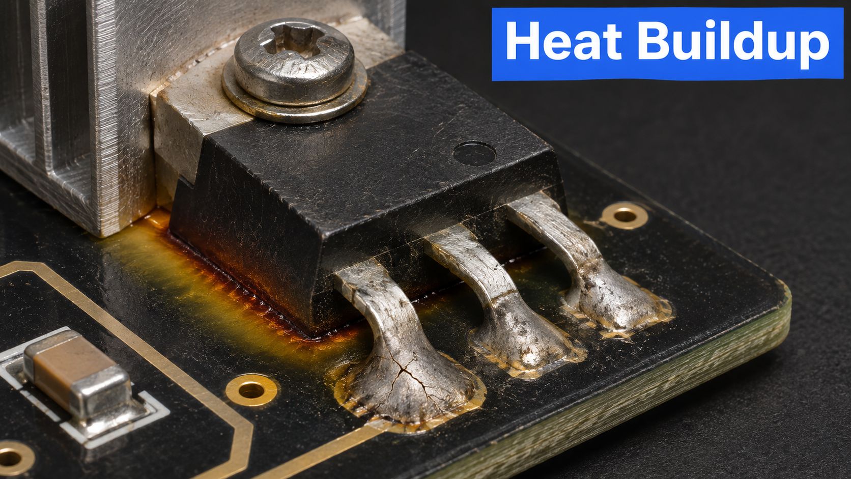
A ceramic board replaces that laminate with a rigid insulating plate bonded to copper, and heat leaves through the plate rather than around it. The entry test is simple: work out the heat flux under the component, and if it pushes the laminate past its rated temperature, the ceramic question is open.
<a id="the-numbers-on-one-stated-basis"></a>
The numbers on one stated basis
A review of alumina and AlN substrate properties reports room-temperature thermal conductivity of about 20 W/m·K for alumina and 160–260 W/m·K for developed AlN substrates, with practical values of 240–260 W/m·K. On that basis AlN moves more than 12 times the heat of alumina. The same review gives AlN's theoretical room-temperature figure as about 320 W/m·K, then explains why almost nobody ships it: oxygen impurities, raw-material quality, density and sintering additives all pull the achieved value down.
A peer-reviewed review of ceramic substrate selection runs the same comparison on a typical basis, 20–30 W/m·K for alumina against 150–230 W/m·K for AlN, a five- to eight-fold improvement. Both ranges are honest. They describe different grades, different measurement methods and different ideas of typical, which is exactly why the word "AlN" on a drawing specifies nothing by itself.
Compare on one basis or not at all. Typical values and developed-substrate values differ by more than the gap between some pairs of materials.
<a id="what-the-conductivity-number-costs-in-handling-and-temperature"></a>
What the conductivity number costs in handling and temperature
The trade-off shows up in your hands before it shows up in simulation. The same review reports AlN bending strength near 300 MPa and fracture toughness around 3–4 MPa·m^1/2, so depanelization, drilling and thermal-shock design need more care than the electrical design suggests.
If you want the failure mode in motion before you commit to a stack-up, the video below is a reasonable ten minutes.
<iframe width="100%" style="aspect-ratio: 16 / 9;" src="https://www.youtube.com/embed/qaH31phG8XM" frameborder="0" allow="autoplay; encrypted-media" allowfullscreen></iframe>Conductivity isn't a constant either. Measured AlN in one technical study fell from about 179 W/m·K at room temperature to 110 W/m·K at 300 °C, which means a 25 °C datasheet value can overstate a material precisely where you need it most.
Ask for the measurement condition, not just the number. A conductivity figure without a test temperature, a grade and a stated method is a marketing claim, and your thermal model will believe it.
<a id="beryllia-and-silicon-nitride-as-niche-substrates"></a>
Beryllia and Silicon Nitride as Niche Substrates
Two materials sit outside the alumina-versus-AlN argument, and both earn their place for reasons that have nothing to do with the top conductivity figure.
Beryllia (BeO) delivers conductivity in AlN's territory while expanding at a rate close to alumina's, which makes it attractive on paper for the highest heat fluxes. It is also toxic in dust form, so machining, scoring, laser processing and scrap handling must run under controlled conditions with extraction and documented procedures. Confirm the shop's dust controls and your local rules for beryllia-bearing waste before it goes on a drawing. Most programs avoid it unless nothing else meets the thermal target.
Silicon nitride (Si3N4) trades conductivity for toughness and a low expansion coefficient. It gives ground to AlN on heat spreading but holds together better under repeated cycling with heavy copper, which is why automotive power modules are its natural home. When qualification is dominated by thermal cycling rather than peak temperature, that trade is usually the right one.
Neither material shares the published dielectric-strength baseline that alumina and AlN carry, so get the value for the specific grade from the datasheet rather than assuming it tracks alumina.
One electrical point belongs here too. AlN combines low dielectric loss with a comparatively low dielectric constant, which is much of the reason RF power amplifiers favour it over alumina.
Selection rule: choose beryllia only when its conductivity is genuinely required and the process can control its toxicity, and choose silicon nitride when cycling reliability outweighs the remaining gap to AlN.
<a id="direct-bonded-copper-and-why-copper-thickness-matters"></a>
Direct-Bonded Copper and Why Copper Thickness Matters
A ceramic plate becomes a circuit when copper is bonded to it, and direct-bonded copper (DBC) is the construction that made that practical. A technical study of DBC substrates describes the process as high-temperature bonding above 1,000 °C, with combined substrate thermal conductivity of roughly 24–180 W/m·K depending on the ceramic, and dielectric strength around 20,000 V/mm.
What that buys you is a substrate that carries serious current while staying an insulator. The architecture gives high current-carrying capability, strong electrical isolation, controlled thermal expansion, low electrical capacitance, and a direct heat path from the semiconductor die into the ceramic. By 2002, a peer-reviewed review was already calling DBC substrates the most important electronic circuit boards for multichip power-semiconductor modules, and crediting them with a major contribution to power-electronics packaging in the decade before.
Thickness is a thermal and a mechanical decision at once. The copper that carries the current also stores most of the expansion mismatch that eventually cracks a joint.
The performance case is settled. Later engineering work reported thermal resistance near 30 mK/W for DBC integrated with a liquid cold plate, which is why automotive power modules, industrial drives, traction inverters and renewable-energy converters all rely on it.
The reliability case is where designs go wrong. Copper expands several times faster than alumina, so every thermal cycle pulls at the bond line. A thin copper layer bonded to alumina gets dragged toward the ceramic's expansion instead of behaving like bulk copper, which steadies the package as a whole but concentrates stress at the copper edges and around the bonded regions. That's why production drawings name copper thickness, bond technology, metallization finish, thermal-cycle qualification and minimum copper-to-edge clearance, and why thermal vias or copper spreaders go in only after you've checked current density and the local stress those edges will see.
<a id="how-to-choose-a-ceramic-substrate-step-by-step"></a>
How to Choose a Ceramic Substrate Step by Step
Seven checks turn the material question into a decision you can defend in a design review. Work them in order; each one produces one of three answers: stay on alumina, move to AlN, or move to silicon nitride.
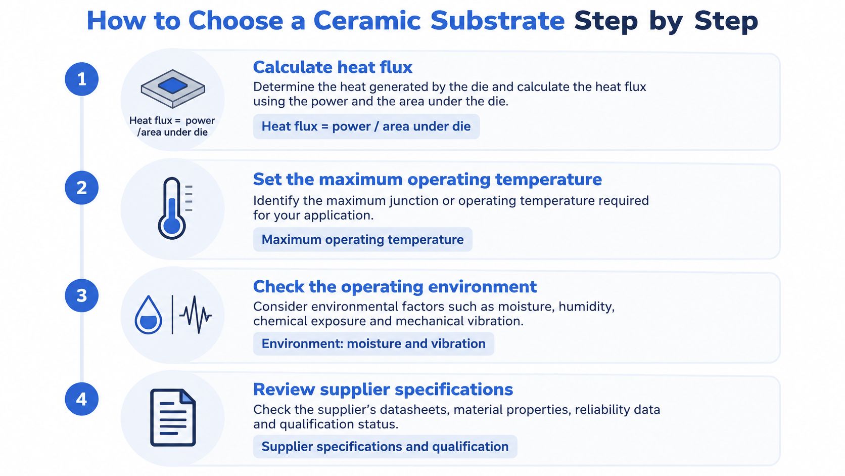
- Calculate heat flux, not total wattage. Divide the power dissipated by the area under the die. A small part throwing a few watts out of a tiny footprint is a harder problem than a larger part spreading more watts over ten times the area, and the density is what decides whether alumina holds.
- Fix the maximum operating temperature and read conductivity there. A figure quoted at 20 to 25 °C describes a bench measurement, not a running inverter. This step tells you whether the grade you picked still meets the target when it's hot.
- Add up total thermal resistance end to end. Die attach, ceramic thickness, copper, interface material and heat sink all sit in series. A short, well-bonded heat path can keep alumina competitive, so this step is where cheap materials survive.
- Check the mechanical limits. Board size, thickness, drilling, depaneling and vibration load all change once the plate is brittle. This is the step that pushes a design from AlN back to alumina, or toward silicon nitride.
- Match copper thickness to current, then check CTE against the package. Thick copper carries more current and stores more mismatch; the package and the solder joint see both.
- Specify dielectric strength with the withstand test voltage and its conditions. Isolation is cheap to over-specify and expensive to discover late.
- Compare full-system cost, including heat-sink volume. A cheaper substrate that forces a bigger enclosure is not cheaper, and this step is where that shows up on the spreadsheet.
The system-level case for AlN is larger than the material gap, and softer than most comparisons admit. Published market analysis of ceramic substrates claims AlN can reduce heat-sink volume by about 35% and improve full-system efficiency by 2–3%, but those figures move with die size, copper thickness, interface resistance, cooling method, metallization and operating temperature. A newer peer-reviewed AlN study measured 182.4 W/m·K, a useful reminder that a production grade can sit well below the headline range.
That's why an inexpensive alumina board can beat AlN economically when the heat path is short or the heat sink is already oversized, while AlN becomes defensible once power density and enclosure volume make cooling hardware the dominant system cost.
<a id="ceramic-material-choice-by-application"></a>
Ceramic Material Choice by Application
| Application | Typical heat load | Usual substrate | Deciding factor | |---|---|---|---| | Low- to mid-power LED lighting | Moderate | Alumina | Cost and brightness per dollar | | High-power LED engines | High | AlN | Junction temperature and lumen maintenance | | Power semiconductor modules and inverters | High | DBC on alumina or AlN | Copper thickness and thermal cycling | | RF power amplifiers | High, localized | AlN | Heat spreading and dielectric loss | | Automotive power electronics | High, under cycling | AlN or silicon nitride | Reliability under thermal cycling | | General-purpose power board | Low to moderate | Alumina | Cost and mechanical strength |
Read the first two rows together, because they're the same product category with different economics. Low- to mid-power lighting is a brightness-per-dollar argument, and alumina or a metal-core PCB usually settles it. High-power LED engines are a junction-temperature argument, and AlN enters when lumen maintenance starts dropping over life.
The middle rows are thermal-cycling problems dressed as thermal-spreading problems. Modules and inverters live or die on copper thickness and bond integrity, RF amplifiers want AlN for spreading plus its low dielectric loss, and automotive assemblies lean on AlN or silicon nitride because the qualification is cycling, not peak temperature.
<a id="a-worked-comparison-at-two-power-levels"></a>
A worked comparison at two power levels
Say a design dissipates 10 W through a die with a small footprint sitting close to a chassis wall. The heat path out of the package is short, the interface is well controlled, and the heat sink is already there for other components. Alumina handles that, and AlN would buy you margin you don't need.
Now scale to a 100 W module sharing one heat sink with three other heat sources. The same substrate choice moves the cooling hardware from a modest extrusion to a finned cold plate with a fan, and that's where AlN's premium gets paid back. The material didn't change; the heat flux did.
The table is a shortlist, not a specification. The same application can need different substrates once heat flux, enclosure volume and cycling duty are known.
<a id="specify-your-ceramic-pcb-material-before-you-order"></a>
Specify Your Ceramic PCB Material Before You Order
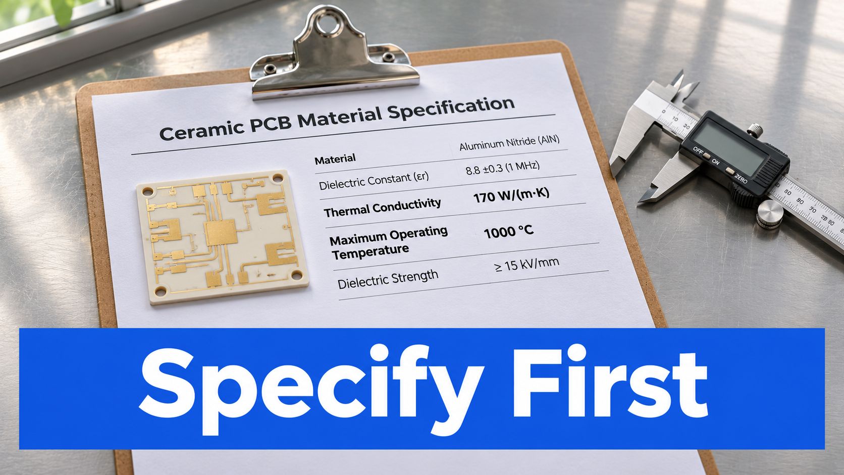
Ten items on a single specification sheet cover almost every failure this material can hand you. Each one exists to prevent something specific.
- Application and maximum operating temperature. This is the basis for every conductivity figure you'll quote, and it stops a board characterized at room temperature from being signed off for a hot enclosure.
- Heat flux, in watts per unit area under the die. It's the item that decides alumina versus AlN, and the one most drawings leave out.
- Substrate material and grade. Alumina at 96%, or AlN with a stated conductivity method and test temperature, never a nominal "AlN" label.
- Substrate thickness. It sets the length of the heat path and therefore the resistance you're paying for.
- Copper thickness matched to current, plus build type. State DBC or thick film explicitly; the two have different rules for clearance, vias and minimum features.
- Bond technology and metallization finish. Both drive solderability and long-term joint reliability.
- Dielectric withstand voltage and the test conditions. A number without conditions can't be verified on receipt.
- Flatness and warpage tolerance. Ceramic handling, stencil printing and reflow all depend on it.
- Minimum copper-to-edge clearance. This controls the edge stress that DBC concentrates during cycling.
- Thermal-cycle qualification and the reliability test that proves the bond survives it. Name the cycle range and the acceptance criteria, not just "qualified".
Cost behaves differently on ceramics than on laminates, because grade, thickness and copper weight move the number far more than board area does. Estimates built on FR-4 area assumptions will mislead you, so check how circuit board price is structured before you budget a prototype run.
This week, fill the sheet in and send it with your drawing for a design-for-manufacture review before you order anything. Copper-to-edge clearance and ceramic handling are the two items that come back changed most often, and both are cheaper to fix on paper. We build ceramic boards on Al2O3, AlN and BeO substrates with DBC and thick-film copper options up to 12 oz, our fabrication is UL recognized and IATF 16949 certified, and we work with RoHS and REACH compliant materials, so the specification you write can be reviewed against real process limits rather than a catalogue page.
A ceramic stack-up that runs cool in the lab and cracks in the field usually failed on copper-to-edge clearance or an unstated test temperature, not on thermal conductivity. Lianyuhong Technology Co.,Ltd builds ceramic PCBs on Al2O3, AlN and BeO with DBC and thick-film copper, and we review dielectric test conditions, flatness and minimum copper-to-edge clearance against your drawing before quoting. Visit Lianyuhong Technology Co.,Ltd with your specification sheet and we'll tell you which of those ten items needs to change.