
The board works on the bench. The Bluetooth link holds across the room, the sensor readings are clean, and the prototype has run for a week without a reset. Then the pre-compliance scan comes back with a peak above the limit near 2.4 GHz, and the schedule now depends on a piece of stamped metal.
This is the moment teams often reach for PCB RF shielding as a fix, and the moment many of them get it wrong. A shield isn't a wall that blocks a frequency. It's a metal box with a resonant frequency, a set of openings that behave like slot antennas, and a return path that has to stay short. Get those three right and the emissions drop. Get them wrong and you've added cost, height and a cavity that rings at exactly the wrong frequency.
Every rule below works as a test rather than a mantra. Instead of memorizing a spacing number and moving on, you'll check it against your own operating band, the harmonics above it, and the route the current takes back to its source.
Table of Contents
- PCB RF Shielding Methods Compared at a Glance
- How RF Leaks From a PCB and What a Shield Blocks
- Aperture Size Limits Set the Real Shielding Performance
- Layout Rules That Keep Return Currents Clean
- How to Build a Grounded Via Fence Step by Step
- Evaluating Shielding Effectiveness Across Frequency
- Confirm Your Shield Design Before Production
<a id="pcb-rf-shielding-methods-compared-at-a-glance"></a>
PCB RF Shielding Methods Compared at a Glance
The first question a product team asks is whether to add a shield can. The better question is which of five common methods matches the board already on the bench.
Board-level work carries a lot of that burden. PCB-level shielding accounted for 41.10% of the global EMI-shielding market in 2024, according to Mordor Intelligence, which says a great deal about how much of the work happens in millimeters rather than in sheet metal.
The table below scores the options against the same criteria, so you can read across a row instead of collecting claims from five different datasheets.
| Method | Best fit | Key spec | Cost and area | Main weakness | |---|---|---|---|---| | Via fence | Multilayer boards with one RF block | Ground ring of vias tied to an internal plane | Low cost, uses a strip along the block | Cavity resonance can raise coupling | | Shield can | Soldered modules such as Wi-Fi or Bluetooth | Continuous solder ring on ground lands | Higher part cost and height | Lid gaps and missing solder leak | | Edge plating | Boards with accessible edges | Plated edges bonded to a ground plane | Moderate cost, less board area than dense stitching | Only as good as edge continuity | | Dense via stitching | Boards where edges are not usable | Vias 1.27 mm (50 mils) or closer | Consumes more board area | Long gaps let return current escape | | Metal enclosure | Whole-product shielding | Sealed seams, filtered cable and vent openings | Tooling and weight cost | Seams, cables and vents dominate leakage |
Read the fence row first if you have four or more layers and a single RF block to isolate. It's the cheapest option and the one whose performance shifts most across the band, which is why the build procedure later gets its own section. Take the shield can row when the radio is a soldered module with a defined ground ring and you need a guaranteed solder ring rather than an approximate one.
Edge plating and dense stitching are substitutes for each other. Choose edge plating when the board outline is accessible to the fabricator and area is tight. Choose dense stitching when the edges are crowded by connectors or the panel is panelized in a way that makes plating awkward.
None of these rows stands alone. Whichever you pick, the laminate sits underneath it, and at millimeter-wave or low-loss bands the dielectric behaviour and the fence geometry get settled together. That's why high-frequency PCB fabrication on Rogers, PTFE or hybrid stack-ups is specified at the same time as the shield rather than after it.
<a id="how-rf-leaks-from-a-pcb-and-what-a-shield-blocks"></a>
How RF Leaks From a PCB and What a Shield Blocks
A board's ground planes and via fences form a metal box around the circuitry. The walls hold. The doors leak: the open edge of the board, the seam where a lid meets its frame, the vent above a power stage, the clearance around the antenna, the trace that runs out to a connector.
That framing tells you where effort pays off. Adding metal where metal already exists changes almost nothing. Closing a gap that sits in the middle of a radiating current path changes a lot. And once you close the box, it becomes a resonant cavity: any internal dimension comparable to a wavelength can ring at its own frequency. So treat the finished shield as a pass or fail test against your operating band, never as a fixed rule that works everywhere.
Why shielding became a board requirement. Digital products sold into major markets carry electromagnetic emissions limits, so any device with clocks and fast edges leaves the factory as a regulated emitter. Compliance moved interference control from a radio-engineering specialty onto every PCB layout review.
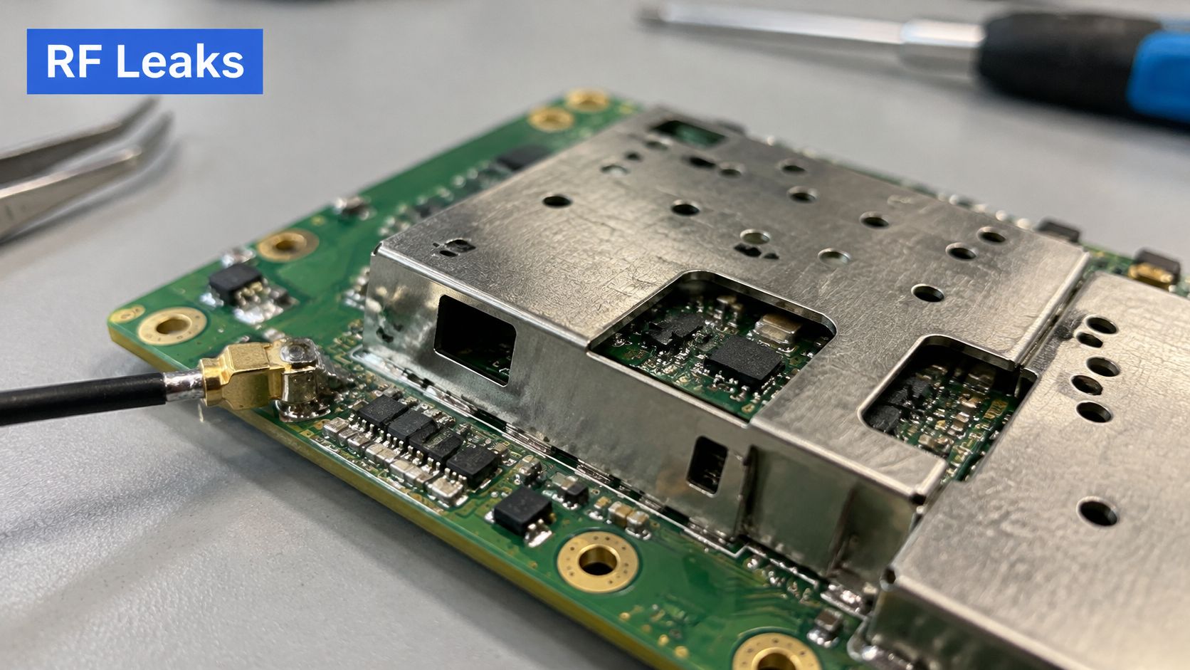
An EMI/RFI design note on board-level shielding gives two figures worth keeping as targets: plastic housings used with microcontroller-based equipment may need at least 40 dB of shielding effectiveness to bring PCB radiation under US or European limits, while a 1 mm sheet-metal enclosure can exceed 100 dB across 1 MHz to 20 GHz provided seams, apertures and cable entry points don't dominate the leakage.
That last clause carries the weight. The gap between a 40 dB result and a 100 dB result is rarely the metal. It is the openings and the bond to ground. A lid measured in isolation and a lid soldered to a stitched ground frame behave like two different products.
Working rule: a shield lid that isn't bonded to a quiet ground plane is a metal hat, not a shield.
Inside the board, four source types do most of the radiating. RF ICs and their power amplifiers couple into nearby traces. Crystal oscillators leak a narrow but stubborn tone at the reference frequency. High-speed buses radiate from the edges of fast clock and data lines. Switching power-stage nodes produce broadband noise up to hundreds of megahertz. A shield contains those sources and blocks incoming coupling, while a noisy connector or an unfiltered cable leaving the enclosure walks straight past it.
Before you choose a method, make two lists. On the left, every radiating source with its frequency and its highest harmonic. On the right, every path that leaves the board: cables, connectors, power entry, antenna feed. The shield only helps where the two lists overlap. A source with no exit path is already contained, and an exit path with no source behind it is a mechanical detail, so spend the shielding budget on the intersections instead of covering the whole board by habit.
<a id="aperture-size-limits-set-the-real-shielding-performance"></a>
Aperture Size Limits Set the Real Shielding Performance
At high frequency an opening stops being a hole and starts being an antenna. A slot cut into a conducting surface radiates efficiently as its longest dimension approaches a half wavelength, and it leaks well before that point. Interference Technology's EMI basics guide puts the practical limit on apertures, seams and grounding continuity rather than on the conductivity of the metal.
The design rule that follows is to keep the longest aperture dimension below one-twentieth of the shortest wavelength, with one-fiftieth as a more conservative target. Work it at 2.4 GHz, where the wavelength is approximately 125 mm. A vent, clearance or shield discontinuity should ideally be no larger than about 6.25 mm, and preferably about 2.5 mm.
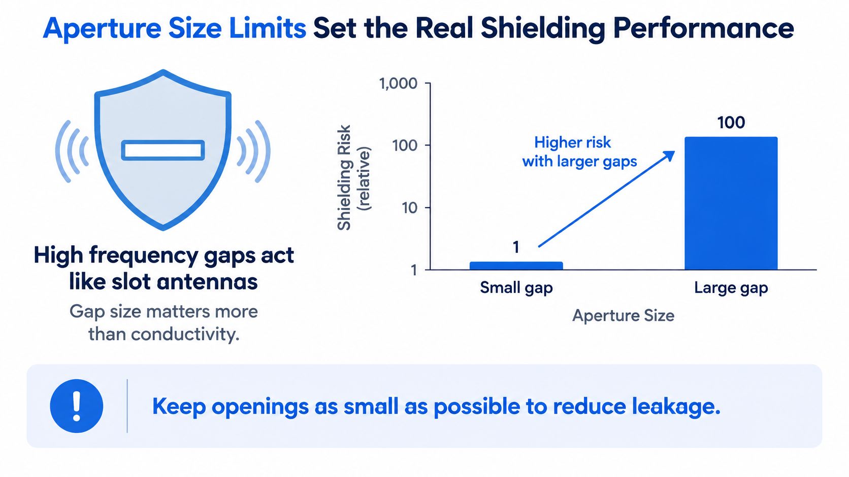
The same arithmetic covers the rest of the band. Wavelength falls as frequency rises, so the limit tightens quickly.
| Frequency | Wavelength | Max aperture (λ/20) | Conservative target (λ/50) | |---|---|---|---| | 2.4 GHz | about 125 mm | about 6.25 mm | about 2.5 mm | | 5.8 GHz | about 52 mm | about 2.6 mm | about 1.0 mm | | 28 GHz | about 10.7 mm | about 0.54 mm | about 0.21 mm |
Now apply it to the harmonic, not just the carrier. A 2.4 GHz radio also emits energy at 4.8 GHz, where the wavelength is about 62 mm, so the λ/20 limit lands near 3.1 mm and the λ/50 target near 1.2 mm. The second harmonic sets a limit roughly half the size of the carrier limit, and the third harmonic is stricter again.
The usual culprits are unglamorous. A lid that sits a fraction of a millimeter off its frame creates a slot the full length of the shield wall. Vent holes punched over a switching regulator form an array of small apertures that leak as a group. Cut-outs for test points and tuning access punch holes exactly where the field is strongest. A long unbroken gap where a trace crosses under the shield boundary turns the whole perimeter into a slot antenna.
Measure the largest continuous gap on the finished layout, then compare it with the row for your highest harmonic. If the gap is bigger, the aperture is the design constraint, not the metal.
<a id="layout-rules-that-keep-return-currents-clean"></a>
Layout Rules That Keep Return Currents Clean
Take a 2.4 GHz sensor board with a crystal, an RF front end, a battery input and a USB port. Every decision that decides whether the shield works is made before any metal arrives. Treat the shielded region as a resonant cavity that the layout either feeds or starves, and each rule below becomes a pass or fail check against your operating band and the return path underneath it.
Put the radiators inside and the ports outside. The crystal and the RF front end belong inside the fence, because they are the sources you are containing. High-speed lines that aren't part of the radio stay outside the boundary or route on a layer far from it, so they never carry noise into the quiet zone. If a noisy trace ends up inside the cavity, the shield holds that energy in and lets it build.
Filter every entry. The battery line crosses the boundary through a pi filter placed as close to the shield wall as the layout allows, with its ground tied to the same plane as the fence. Every conductor that enters the shielded region is a leak path until you filter it, because an unfiltered wire passing through the wall couples the cavity straight to the outside world.
Move the USB connector to the board edge, outside the fence, and tie its ground to the same plane. If the return current from that connector has to travel around the shielded region to reach its source, it couples into everything it passes. The cable then radiates whatever it picked up along the way.
Texas Instruments' shielding white paper is blunt about where fences fail: a via fence can become ineffective when it sits far from the source, when it is interrupted by long gaps, when it connects to a noisy copper island, or when it forces return current through a route you didn't intend.
Fence placement beats fence density. Current follows the path of least impedance, and the plane beneath the fence sets that path, so via count alone fixes nothing.
Edge treatment is a real decision with a real price. Plated board edges generally shield better than via stitching alone and consume less layout area, while adding process cost per panel. Pay for plating where the measurement shows it buys isolation you need, and accept a well-built fence everywhere else.
The practical task is one page of drawing. Outline the shield boundary on the layout, then list every signal, power line and cable that crosses it, with the filter and the return path for each. Anything on that list without a filter is a leak you've already designed in. The return-path discipline behind high-speed PCB design applies directly to shielded RF regions, because a clean return is what keeps the cavity quiet in the first place.
<a id="how-to-build-a-grounded-via-fence-step-by-step"></a>
How to Build a Grounded Via Fence Step by Step
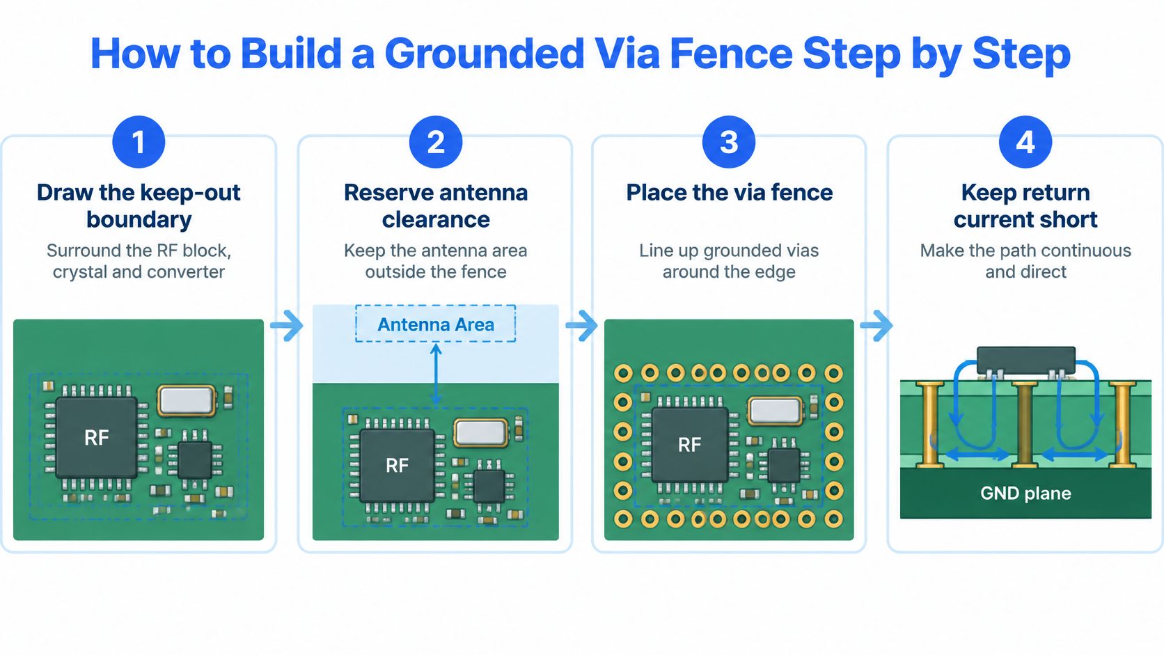
A grounded via fence connects the surface ground pour to the internal reference planes and forms a conductive vertical boundary around a sensitive block. The goal for every step below is the same: keep the return current short and continuous.
-
Draw the keep-out boundary first. Outline the RF block, the crystal and any switching converter on the top layer before you place parts, then reserve antenna clearance outside that line so the fence doesn't sit in the antenna's near field and detune it.
-
Lay a continuous ground land along the boundary. No signal trace crosses beneath it. A broken land forces return current onto a longer path, and a longer path is a loop antenna.
-
Space stitching vias at 1.27 mm (50 mils) or closer and tie them to an unbroken internal ground plane. A handful of widely spaced vias presents a high-inductance return, so the metal ring exists on paper but not electrically.
-
Close every gap in the ring. One long gap lets current take an unintended route around the fence, and the fence then shields the wrong region.
-
Keep the reference plane under the fence solid. Avoid splitting it beneath sensitive transitions. A split plane forces the return current to detour, and every detour is coupling you can't simulate away.
-
Keep the fence close to the source and off noisy copper islands. Proximity matters more than density, and a fence tied to a noisy island injects the noise it was meant to contain.
-
Simulate with the actual stack-up before release. Include the shield can, the seams, and the connectors in the model. A field solver run on the bare board tells you about the wrong structure.
Here's the part that changes how you sign off. A peer-reviewed study in the Journal of the Institute of Electronics Packaging examined how via fences affect signal-via transitions inside shielded regions and found the effect is frequency dependent. The fence improved performance below approximately the lowest cavity-resonance frequency by forming vertical ground surfaces, but could strongly degrade performance at cavity resonances.
The board doesn't have a shield problem at those frequencies. The planes, vias and dielectric spacing form a cavity, and the cavity rings. Adding vias doesn't lower coupling; it can create resonant modes that raise it at particular frequencies. The fence is useful for isolating functional units and reducing interaction between the board and surrounding objects, and resonance can reverse that benefit.
A finished fence looks boring in review: one closed ring, uniform spacing, a solid plane underneath, and no trace crossing the line. Write the pitch, the plane layer and the resonance check into the review record so the next revision doesn't reopen the ring.
<a id="evaluating-shielding-effectiveness-across-frequency"></a>
Evaluating Shielding Effectiveness Across Frequency
A single low-frequency test can pass while the shield fails badly elsewhere. Modeling of PCB shields reported roughly 38 to 44 dB of shielding at 850 MHz in one configuration, with isolation reaching 86 to 92 dB for selected component placements. Shielding effectiveness then fell to about 28 dB at 1.9 GHz, and negative shielding was observed near 2.1 GHz when structural dimensions aligned with resonant conditions, as described in In Compliance Magazine's modeling study.

That negative figure is the one to remember. A shield that concentrates field energy into a resonant mode makes emissions worse than no shield at that spot, and the only way to know is to measure across the band.
Set a dB-versus-frequency target before you test, covering carrier, harmonics, clock edges and switching-converter noise. Then run the checks in the order below rather than jumping straight to the chamber, because each stage removes a class of failure the next stage would have charged you to find.
| Stage | When to run it | What it reveals | Typical equipment | |---|---|---|---| | Pre-layout return-path review | Before component placement | Distant fences, long gaps and noisy islands | Stack-up and layout review | | 2.5D or 3D simulation | After layout | Seam, connector and shield-can leaks | Electromagnetic field solver | | Near-field probing | First prototype | Location of leakage hot spots | Near-field probe and spectrum analyzer | | Conducted and radiated EMC testing | Pre-compliance and certification | Total product emissions with cables and enclosure | Pre-compliance or accredited chamber |
Near-field probing earns its place early. Scanning the first prototype moves the hunt for leakage from a paid chamber slot to your own bench, and it usually finds the one seam or cable that dominates everything else.
Build the test sample to production reality. Include assembly tolerances, lid contact resistance, cable routing and the worst-case clock configuration. A shield that measures well on a bare board with the lid resting in place can leak once it's soldered down and enclosed.
The measurement chain starts below the shield. Impedance control on the RF traces decides how much energy reaches the boundary in the first place, and a stack-up that shifts impedance across the lot will shift your emissions with it.
Keep isolation and compliance separate in your head. Isolation between two RF blocks is a locally measurable number, and a shield can improve it while a connector or cable stays the dominant radiator for the product as a whole. Pass the local test and fail the system test, and the shield wasn't the problem.
For a look at the measurement side of this work, the video below walks through the practical side of evaluating a shielded design.
<iframe width="100%" style="aspect-ratio: 16 / 9;" src="https://www.youtube.com/embed/-S8O9Gr_z7o" frameborder="0" allow="autoplay; encrypted-media" allowfullscreen></iframe>Test rule: if your shield specification doesn't name a frequency band, you don't have a specification. You have a shape.
<a id="confirm-your-shield-design-before-production"></a>
Confirm Your Shield Design Before Production
Run this list before the layout goes to fabrication. A board that fails any item goes back to layout, not to the test bench, because a test only tells you what the layout already decided.
-
State the highest frequency and harmonic the shield must handle. Confirm every aperture is below the matching row in the aperture table. The harmonic sets the stricter target, so a 2.4 GHz design is judged at 4.8 GHz and above.
-
Confirm stitching vias are 1.27 mm (50 mils) or closer and tied to an unbroken internal plane. Verify on the fabricated cross-section, not just in the design file.
-
Confirm no signal crosses the shield boundary, and that every cable and power entry has a filter with a return path to the same plane.
-
Confirm the simulation included seams, connectors and the shield can, and that the test plan covers near-field probing plus conducted and radiated testing with the final enclosure.
-
Settle the substrate question before the first build. If the design needs a high-frequency laminate, agree the material and the verification method up front. We quote Rogers, PTFE and high-speed materials with low Dk/Df values and verify them with SET2DIL, Delta-L and VNA testing, and every board is manufactured to IPC-2 or IPC-3 standards with 100% AOI, flying probe and electrical testing.
-
Write the shield specification on one page. Frequency target, aperture limit, fence spacing, filtered entries, and the test that counts as proof. One page is enough because every line traces back to a number you've already checked.
The last item is the one that keeps a program honest. When the specification, the layout and the test plan all quote the same band and the same limits, a failing scan points to a specific seam or a specific trace instead of a vague argument about whether the shield is good enough.
Lianyuhong Technology Co.,Ltd builds the high-frequency boards these shields sit on, using Rogers, PTFE and high-speed laminates with documented stack-ups and SET2DIL, Delta-L and VNA verification, then assembles the shield can and the parts beneath it in the same turnkey flow. Send us your stack-up, your operating band and the harmonic you need to clear, and our engineers will review the fence spacing, aperture limits and ground ring against your layout before release. Visit Lianyuhong Technology Co.,Ltd to start the review.