
A connector that feels solid in your hand can still hide a hollow solder barrel. That's the central lesson of through hole PCB assembly. The lead gives you strength, but only if solder wets the barrel wall and the copper plating survives every heat cycle you put it through. Get those two things right, and a through-hole joint will outlast connectors, cables, and repeated handling. Get them wrong, and you'll chase intermittent opens that no visual inspection caught.
Table of Contents
- What Through-Hole PCB Assembly Is and Why It Persists
- Through-Hole Versus SMT and Mixed Boards
- Hand Insertion Wave and Selective Soldering
- Hole Geometry and Solder Fill Rules
- Tests That Prove a Through-Hole Joint
- Where Through-Hole Parts Earn Their Keep
- Choose an Assembler and Send the Right Files
<a id="what-through-hole-pcb-assembly-is-and-why-it-persists"></a>
What Through-Hole PCB Assembly Is and Why It Persists
MarketIntelo reported that through-hole technology (THT) assembly represented $11.2 billion, or 13.1% of the global PCB assembly market, in 2025. That share tells you this isn't a legacy process kept alive for hobby boards. It's a deliberate choice for parts that need to stay put.
Say you're building a motor drive. The controller IC and passives are tiny surface-mount parts. The screw terminal block on the edge isn't. A technician will push wires into it, tighten screws, and pull cables sideways for years. If that block sits only on surface pads, each tug levers against a thin fillet. Put its pins through the board and solder them on the far side, and the load spreads through the full board thickness.
<a id="the-rivet-picture"></a>
The Rivet Picture
Think of the joint as a rivet. The component lead is the shank. The plated barrel, the copper-lined hole through the board, is the hole it locks into. Solder forms the head on the opposite side and fills the gap between shank and barrel in between.
That one structure does two jobs at once. Electrically, solder connects lead to barrel to traces on other layers. Mechanically, the lead can't lift off the way a surface pad can, because it's captured through the board.
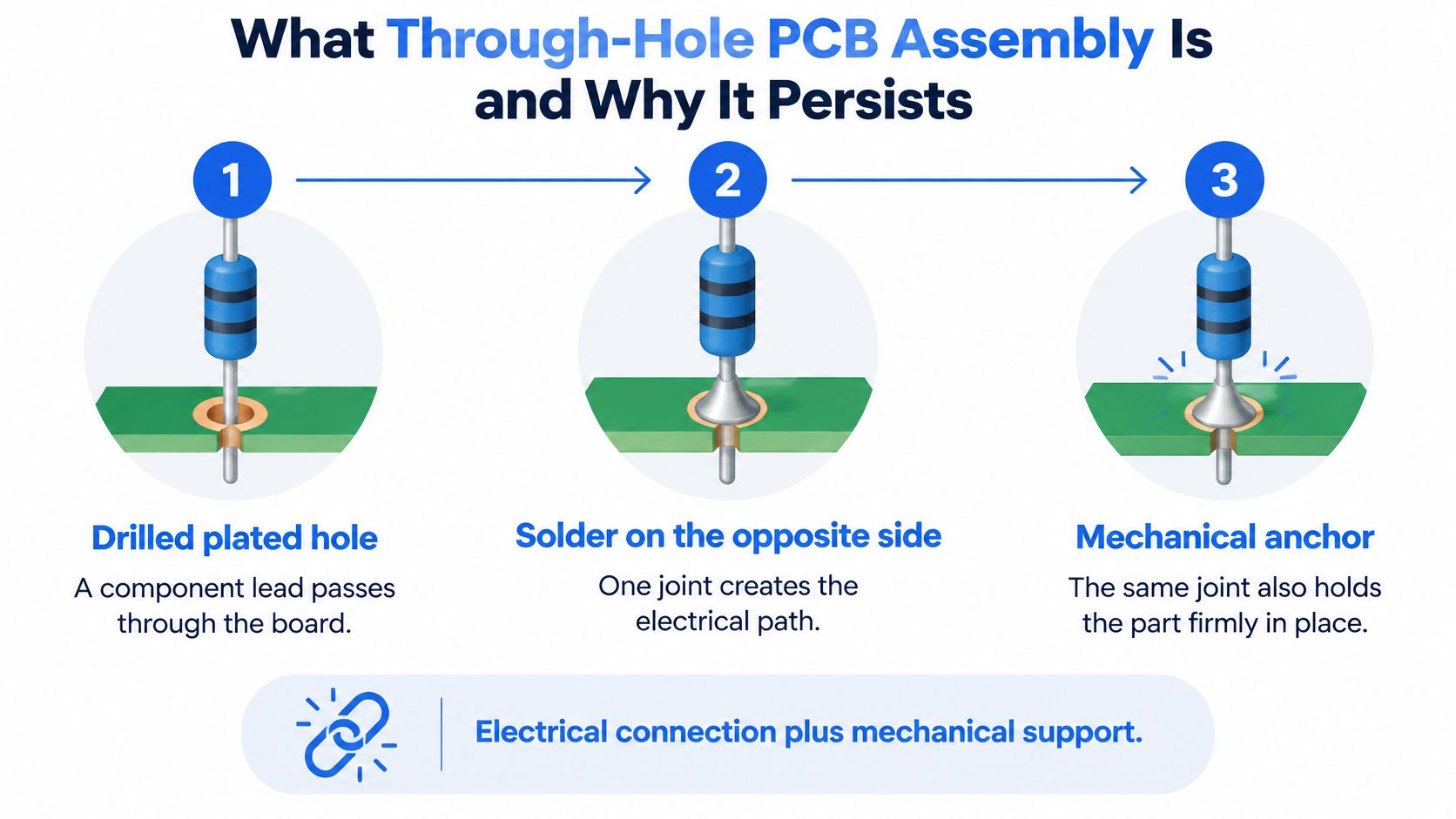
The workflow behind that picture has three steps:
- Drill the board with finished, plated holes sized for each lead.
- Insert the component leads through those holes from one side.
- Solder each lead to its pad and barrel on the far side.
<a id="parts-that-still-need-the-anchor"></a>
Parts That Still Need the Anchor
You'll keep seeing the same categories in through-hole: board-edge connectors that get mated and unmated, transformers with real mass, relays, large electrolytic capacitors, and power devices that carry high current or bolt to a heatsink. They share one trait. Something pulls, pushes, vibrates, or heats them in service.
There's a geometric cost, and it's simple. Every lead consumes a drilled hole plus a routing keep-out on every layer it passes through, so the rest of a modern board usually goes to surface mount. You spend board area only where the anchor earns it.
The choices that follow flow from that trade. You'll decide which parts stay through-hole and which go SMT, pick hand, wave, or selective soldering, set hole and fill rules, test what you can't see, and cost the result. Keep one caveat in mind throughout. The anchor is only as strong as the copper barrel and the solder inside it.
<a id="through-hole-versus-smt-and-mixed-boards"></a>
Through-Hole Versus SMT and Mixed Boards
Start with the table, because most placement arguments end here.
| Criterion | Through-hole | Surface mount | Mixed technology | |---|---|---|---| | Mechanical load | Lead through the board anchors the part | Surface fillet; weak in pull and shock | Loaded parts in through-hole; ICs in SMT | | Board space | One drilled hole and keep-out per lead | Pads only, including 01005 and fine-pitch BGA | SMT density plus a few through-hole sites | | How it is soldered | Hand, wave or selective | Reflow, often in nitrogen | Reflow first, then wave or selective for leads | | Best fit | Connectors, transformers, relays, power parts, low volume | Dense digital, RF passives, high volume | Most shipping products | | Main risk | Hollow barrel or cracked plating despite a strong lead | Pad lift or weak mechanical hold | Second heat cycle and keep-out around SMT |
Mechanical load is the row that decides most boards. A through-hole lead resists pull-out because solder locks it along the barrel, not just at a surface pad. If users will mate a cable to it or the part is heavy, that row wins.
Board space runs the other way. A peer-reviewed review of PCB technology reports that through-hole technology was the dominant component-mounting method in the 1950s, while surface-mount technology became mainstream in the 1980s and SMT reduced electronic package size, cost, and complexity. That's why logic, chip passives, and fine-pitch packages belong on pads. If you're placing dense devices, our guide to BGA PCB assembly considerations covers the pad and reflow side of that decision.
How it is soldered matters because the two technologies melt at different stages. SMT parts are placed in paste and reflowed. Through-hole leads are soldered afterward by hand, wave, or a selective nozzle. You can't casually run both through one process and hope for the best.
Best fit follows from the rows above it. Connectors, transformers, relays, and power parts stay through-hole. Dense digital and RF circuits stay SMT. Neither technology wins across a whole product.
Main risk is the row teams underestimate. A through-hole board can fail inside the barrel while the part feels rock solid. An all-SMT board can fail at the pad when a connector gets pried sideways. Mixed boards avoid both failures but introduce a second heat cycle you have to manage.
<a id="how-mixed-boards-are-actually-built"></a>
How Mixed Boards Are Actually Built
Mixed technology is the normal modern board, not an exception. The assembler reflows SMT parts first, on one or both sides. Operators or insertion equipment then place through-hole parts, and those leads get soldered without remelting nearby SMT joints.
Double-sided SMT plus a row of connectors is the case that breaks a simple wave process. A full solder wave would wash over bottom-side SMT parts, so shops use wave pallets that mask everything except the leads, or they switch to selective soldering and touch only the through-hole sites.
If the part is inserted, mated, or carries high current and mass, keep it through-hole. If it's small, numerous, or fine-pitch, keep it SMT.
Apply that rule part by part on your bill of materials. You'll end up with a short through-hole list and a long SMT list, which is exactly what a shippable mixed board looks like.
<a id="hand-insertion-wave-and-selective-soldering"></a>
Hand Insertion Wave and Selective Soldering
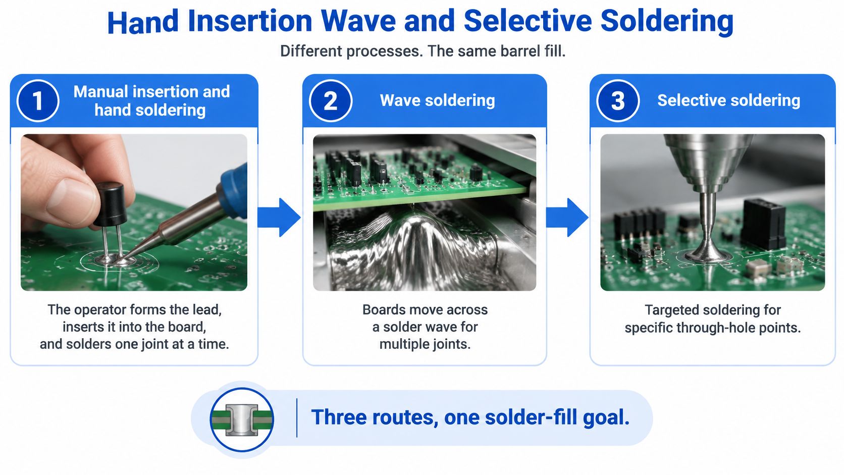
These three processes aren't quality ranks. They're three ways to deliver the same thing, a filled barrel, at different volumes and board layouts.
| Process | How the joint is made | Best fit | Limit to design for | |---|---|---|---| | Hand solder | Lead formed, inserted and soldered one joint at a time | Prototypes, rework, a few large parts | Operator variation and slow throughput | | Wave solder | Flux, preheat, then a solder wave on the bottom side | Many leads, mostly single-sided through-hole | SMT must be masked; thermal shadows under big parts | | Selective solder | Programmed nozzle or mini-wave on chosen sites | Mixed boards with SMT near connectors | Nozzle keep-out and annular-ring heat balance | | Lead-free example | 285°C pot, 120°C preheat, 9 to 11 seconds contact | RoHS builds and rework planning | Plastics, electrolytics, LEDs and relays versus max temperature |
<a id="hand-soldering-fits-a-handful-of-joints"></a>
Hand Soldering Fits a Handful of Joints
An operator forms the lead, inserts it, trims it, and solders one joint at a time with an iron. That's the right answer for prototypes, odd mechanical parts that won't feed through equipment, and rework. It's also slow and skill-dependent. Once you're past a few dozen joints per board, variation between operators becomes your defect source.
<a id="wave-soldering-fits-many-leads-on-one-side"></a>
Wave Soldering Fits Many Leads on One Side
Boards move on a conveyor through flux, then preheat, then across a standing wave of molten solder that contacts the bottom side. Every exposed lead gets soldered in one pass. It's fast when many leads share that side, but bottom-side SMT parts need glue or a pallet so they aren't washed off, and large parts cast thermal shadows that leave the pins behind them underfilled.
<a id="selective-soldering-fits-mixed-boards"></a>
Selective Soldering Fits Mixed Boards
A programmed nozzle or mini-wave visits only the sites you choose. SMT parts a few millimetres away stay untouched. This is the usual answer when connectors sit close to dense SMT. The cost is programming time and a nozzle keep-out you must respect in layout.
Press-fit is the no-solder cousin worth knowing. Some backplane connectors use compliant pins that grip the barrel by friction alone. It avoids heat entirely, but it demands tight hole tolerances.
<a id="the-lead-free-heat-check"></a>
The Lead-Free Heat Check
Don't judge a part by its electrical rating alone. An independent lead-free case study shows a lead-free through-hole process using a 285°C solder pot, 120°C board preheat, and 9 to 11 seconds of solder contact. Check heat-sensitive plastics, electrolytic capacitors, connectors, relays, LEDs, and large thermal-mass parts against that dwell, and ask for a recorded profile rather than nominal machine settings.
The alloy label itself isn't the risk. The same source reports a controlled study found no statistically significant difference in mean defects between lead-free and tin-lead assembly across OSP, ENIG, and immersion-silver finishes, and reported successful lead-free through-hole rework. Repeated heat exposure is what you manage.
Match the row to your board. Hand for a handful of joints, wave for a lead-heavy single side, selective when SMT must stay untouched.
<a id="hole-geometry-and-solder-fill-rules"></a>
Hole Geometry and Solder Fill Rules
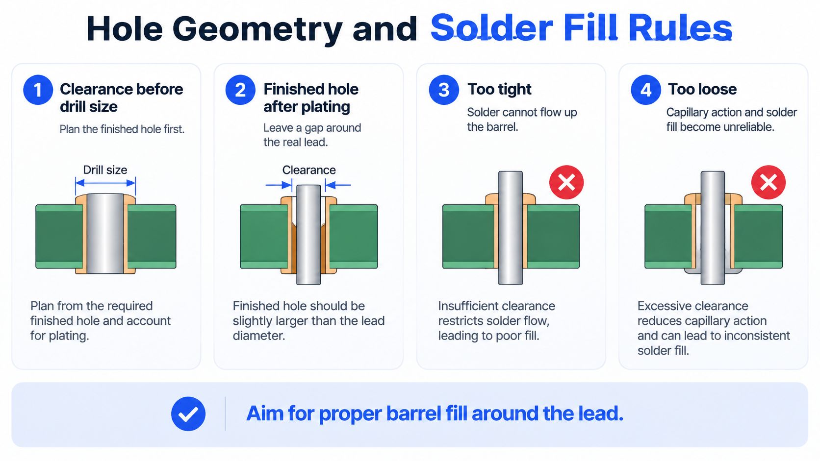
Design the clearance first, and the drill size second. Most fill problems are geometry problems that were locked in at layout.
| Rule | What to set | Check on the drawing | |---|---|---| | Finished hole | Set from maximum lead diameter plus plating and fabrication tolerance | Call out finished size, not nominal drill | | Clearance | Too tight blocks solder flow; too loose starves capillary fill | Check clearance against the actual lead | | Annular ring | Larger land feeds heat into the joint in wave or selective soldering | Balance land size for the chosen process | | Opposite-side copper | Large pour sinks heat and leaves a dull, incomplete fillet | Limit copper pours next to barrels | | Plane-connected hole | Thermal relief balances heat; 50% fill allowed in defined cases | Confirm the allowance against the IPC-A-610 class | | Selective nozzle keep-out | Heat must reach the barrel without spreading into nearby SMT | Mark keep-out on the layout | | Lead protrusion | Protruding length sets wetted length and pull strength | Specify protrusion on the assembly drawing |
<a id="too-tight-and-too-loose-both-fail"></a>
Too Tight and Too Loose Both Fail
The finished hole is what's left after plating, and it must leave a gap around the lead. The EN IEC 61188-6-1 land pattern standard frames joint quality around the clearance between the component lead and the plated-hole wall, not nominal drill size. If the hole is too tight, solder can't flow up around the lead. If it's excessively oversized, capillary action and available solder volume can't fill the barrel.
Work from the maximum lead diameter on the component datasheet, not the typical value. Add plating thickness and your fabricator's tolerance. Then write the finished hole diameter on the fabrication drawing so nobody has to guess what drill produces it.
<a id="the-annular-ring-is-a-heat-pad"></a>
The Annular Ring Is a Heat Pad
The annular ring is the copper land around the hole, and it controls heat as much as connection. A larger land feeds heat into the joint during wave or selective soldering, which helps solder climb the barrel. A huge copper pour on the opposite side does the reverse. It acts as a heat sink, pulls energy away, and leaves a dull, incomplete fillet.
For holes tied to power or ground planes, use thermal relief spokes instead of a solid connection. You keep the electrical path while limiting how fast the plane steals heat. For selective nozzles, balance the land so heat reaches the barrel without spreading into adjacent SMT pads.
Design note: A pretty top-side fillet doesn't prove the barrel filled. Protrusion, flux activity, preheat, and solder contact time decide what happened inside the hole.
<a id="five-checks-for-your-next-layout"></a>
Five Checks for Your Next Layout
Run these before you release files:
- Finished hole from the actual lead, using maximum diameter plus plating and tolerance.
- Annular ring sized for the process you'll use, wave or selective.
- Thermal relief on plane connections, so the barrel can reach wetting temperature.
- Lead protrusion called out on the assembly drawing, since wetted length drives pull strength.
- IPC class written on the drawing, Class 2 or Class 3, so the fill expectation isn't negotiable later.
For connectors and relays on vibrating equipment, add lead forming, staking, or a mechanical bracket to that drawing. Solder shouldn't be the only thing absorbing the load.
<a id="tests-that-prove-a-through-hole-joint"></a>
Tests That Prove a Through-Hole Joint
A board can pass a visual check and a functional test while the barrel is half empty. The net conducts today. The question is whether it still conducts after thermal cycling and vibration, and that takes different evidence.
| Check | Figure | How to use it | |---|---|---| | Class 2 vertical fill | 75% of the barrel | Usual IPC-A-610 acceptance for commercial product | | Class 3 vertical fill | 75% of the barrel | Same headline fill; tighter workmanship around it | | Plane-connected hole | 50% allowed in defined cases | Thick copper planes steal heat from the barrel | | SAC305 thermal-cycle study | No failures through 535 cycles at 25% fill or more | Partial fill can survive; it does not replace the Class target | | Pin wetting in that study | At least 15% penetration, 0.030 inches in the test | Wetted length tracks pull strength better than a top fillet | | Fill-level experiment | 20, 40, 60, 80 and 100% compared | More fill changed stress; model and tensile test differed by 3.39% |
<a id="reading-the-numbers-without-misusing-them"></a>
Reading the Numbers Without Misusing Them
Published reliability work summarized in a study of lead-free through-hole joint reliability notes that IPC-A-610 acceptance criteria commonly require 75% vertical solder fill for Class 2 and Class 3 products, with a 50% allowance for certain plated through-holes connected to power or ground planes. That's your acceptance line. Build to it.
The research figures below that line are context, not permission. Partially filled joints surviving hundreds of cycles tells you a slightly underfilled joint isn't automatic scrap. It doesn't tell you to specify less fill, because your product's board thickness, copper weight, and vibration profile aren't the test vehicle.
The most useful finding is about wetted length. Pin-wetted length correlates with pull strength across different PCB thicknesses, and shock and vibration were the most damaging stresses evaluated. So measure how far solder climbed the pin, and validate products that shake under the load they'll really see.
<a id="match-each-test-to-what-it-can-see"></a>
Match Each Test to What It Can See
- Visual inspection, top and bottom: Catches wetting, protrusion, and fillet shape. Can't see inside the barrel.
- AOI: Confirms presence, polarity, and obvious solder defects at speed. Can't judge internal fill.
- X-ray: Reveals fill and voiding where a connector body hides the joint. Use it on hidden barrels, not every pin.
- Microsection: Destructive, and it's the only method that directly shows barrel cracks and true fill percentage. Use it on a first-article sample.
Add process proof to product proof. Ask for a recorded thermal profile from thermocouples on a real board, not the machine's setpoint screen. Set a written rework limit, because each extra heat cycle can damage barrel copper before the circuit ever opens.
Electrical and functional test confirm the board works now. They don't prove the barrel survives next year. Before you request a quote, name your IPC class, your fill expectation, and whether you want X-ray or a first-article cross-section.
<a id="where-through-hole-parts-earn-their-keep"></a>
Where Through-Hole Parts Earn Their Keep
Abstract rules get easier when you attach them to products you've probably built.
<a id="four-boards-four-reasons"></a>
Four Boards, Four Reasons
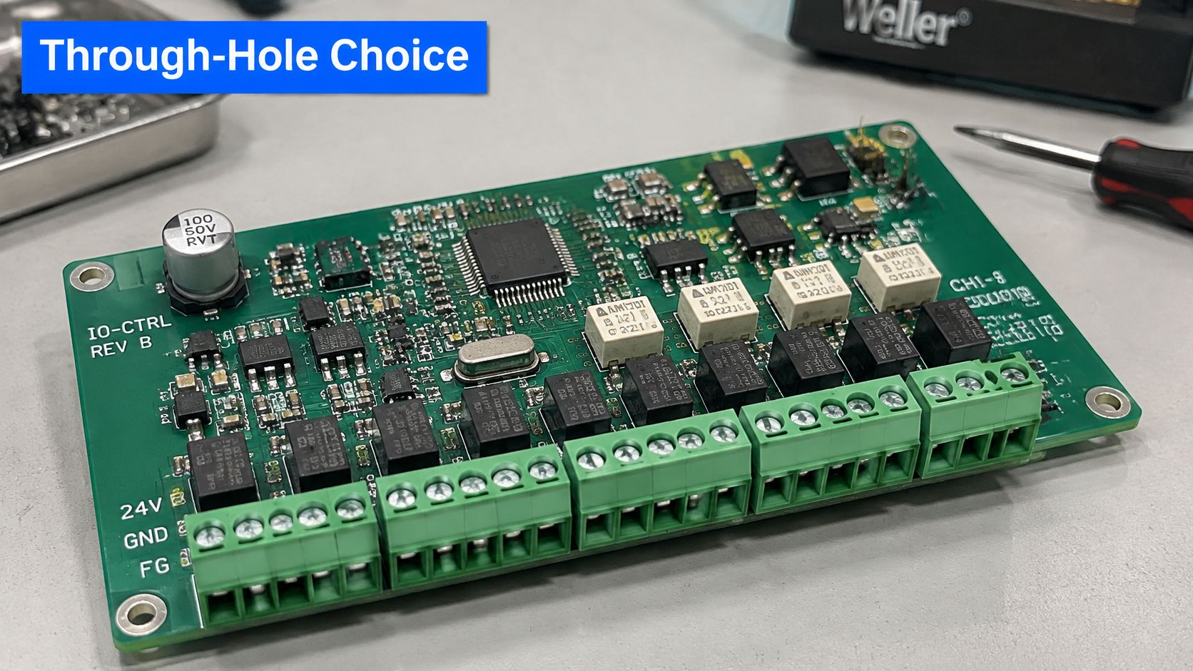
An industrial I/O board puts a dense SMT microcontroller and isolation circuits on top, then a row of pluggable terminal blocks in through-hole. Field technicians will yank those wires. Selectively solder the blocks, and stake them if the enclosure vibrates. Your cost driver is selective programming, paid once per design.
A power supply keeps large electrolytics, a transformer, and a heatsink-mounted MOSFET in through-hole for mass and current, while the control IC stays SMT. The transformer's bulk shadows nearby pins during soldering, so profile those joints specifically. Drilled, plated holes add fabrication time here, and lead time waits on the transformer.
A USB or board-to-board connector on a consumer product goes through-hole or hybrid because mating cycles lever surface pads off the laminate. Everything around it stays SMT to save area. Similar thinking drives connector choices in vehicle electronics, where our automotive PCB manufacturing overview shows how vibration shapes assembly decisions.
A five-board prototype run flips the math. Hand insert the few leads rather than programming a selective nozzle. Labor per joint is higher, but you skip setup and ship sooner once parts are in hand.
Now the contrast. A fine-pitch BGA surrounded by 01005 passives should not be through-hole. Drilled holes would wreck the routing channels under the package and cut yield for zero mechanical benefit.
The video below shows through-hole insertion and soldering at production pace, which helps explain why per-joint cost drops when many leads share one process.
<iframe width="100%" style="aspect-ratio: 16 / 9;" src="https://www.youtube.com/embed/hYvimEqs6no" frameborder="0" allow="autoplay; encrypted-media" allowfullscreen></iframe><a id="pricing-the-choice-in-three-questions"></a>
Pricing the Choice in Three Questions
Ask any shop the same three things. What's the per-joint labor for hand insertion? What's the single-pass wave cost when many leads share one side? What's the one-time setup for selective programming or a wave pallet?
For a prototype, request a hand-insertion quote and a selective quote on identical files and compare line by line. Before either quote, list every through-hole reference designator and write one sentence on why it isn't SMT. If you can't write that sentence, move the part.
<a id="choose-an-assembler-and-send-the-right-files"></a>
Choose an Assembler and Send the Right Files
Don't compare quotes until each assembler answers the same questions. A low price on an undefined process isn't a saving.
<a id="questions-that-reveal-real-capability"></a>
Questions That Reveal Real Capability
- Soldering range: Can you hand solder, wave solder, and selectively solder, or do you only place SMT?
- Thermal evidence: Will you record a measured profile for lead-free through-hole joints on our board?
- Workmanship class: Which IPC class do you build to, and is it written on the traveller?
- Hidden-joint inspection: Is X-ray available, and can you microsection a first article if we ask?
- Rework limit: How many heat cycles do you allow on one barrel before you scrap or escalate?
Our own line is a useful benchmark for what to expect. Our assembly capabilities include nitrogen reflow, wave and selective soldering, SMT from 01005, BGA from 0.35 mm pitch, and through-hole for connectors and power parts, so mixed boards stay under one roof instead of moving between shops.
<a id="pick-the-engagement-model-on-purpose"></a>
Pick the Engagement Model on Purpose
We offer three assembly engagement models, and the right one depends on who should carry sourcing risk. Full turnkey means we fabricate, buy parts, and assemble. Consigned full-kit means you supply boards and components while we assemble and keep records. Partial turnkey splits it, so you supply some parts and we source the hard-to-find ones.
Timing follows parts, not promises. Our prototype turnkey assembly can ship in 24 hours when components are in stock, standard builds take 2 to 5 business days, and volume production typically takes 7 to 15 business days depending on component availability and board complexity. If you're still iterating, our PCB prototype assembly service explains how quick-turn builds are structured.
<a id="the-file-package-to-send-together"></a>
The File Package to Send Together
Send Gerbers, a BOM with manufacturer part numbers, pick-and-place data for the SMT side, and an assembly drawing marking through-hole polarity, lead protrusion, and any staking. Add the solder alloy, the IPC class, and your test list in the same package.
Ask for DFM comments on finished hole sizes and selective keep-outs before you approve the quote. Lianyuhong Technology Co.,Ltd is one supplier to measure against this list. Confirm capabilities, lead times, and location directly before you rely on them for a production date.
Send us your Gerbers, BOM, and assembly drawing, and we'll review finished hole sizes, selective keep-outs, and fill expectations before quoting your mixed SMT and through-hole build. Visit Lianyuhong Technology Co.,Ltd to start a turnkey, consigned, or partial-turnkey assembly quote with wave and selective soldering under one quality system.