
The 01005 component size that most assembly notes mean is about 0.4 mm by 0.2 mm, or 0.016 by 0.008 inch, which metric catalogs file under the code 0402. Some drawing sets use the same 01005 label for a smaller body of 0.25 by 0.125 mm, so the code alone doesn't settle the outline.
That gap between one label and two bodies is where the trouble starts. A footprint drawn from the wrong reading fails in a way that looks like a process problem: parts stand up in reflow, joints starve, inspection passes boards that shouldn't ship. The fix isn't exotic. It's knowing three separate sizes, the body, the code and the copper, and treating each as its own decision. A resistor and a capacitor in the same outline can need different land patterns, different nozzles and different 3D bodies in the CAD library, and none of that appears in the package code.
Table of Contents
- 01005 Body Size in Millimetres and Inches
- Why 01005 and Metric 0402 Collide
- Land Patterns That Fit the Tiny Body
- How Paste Placement and Inspection Must Change
- When to Use 01005 and When to Stay on 0201
- Confirm the Footprint Before You Build
<a id="01005-body-size-in-millimetres-and-inches"></a>
01005 Body Size in Millimetres and Inches
Four 01005 bodies cover about the same board rectangle as one imperial 0201. Most assembly notes that say 01005 mean a body about 0.4 mm long by 0.2 mm wide, which converts to 0.016 by 0.008 inch. The component-selection notes published by PCD&F give those nominal dimensions, put resistor height near 0.1 mm and capacitor height near 0.2 mm, and record pad-to-pad spacing of roughly 0.13 mm, or 5 mils, with 1,000 pieces weighing about 0.04 gram.
| Measure | 01005 (common assembly use) | 0201 imperial reference | |---|---|---| | Length | 0.4 mm (0.016 in) | 0.6 mm | | Width | 0.2 mm (0.008 in) | 0.3 mm | | Resistor height | About 0.1 mm | No code-fixed nominal height; it is part-specific | | Capacitor height | About 0.2 mm | No code-fixed nominal height; usually taller than the resistor | | Pad-to-pad spacing | About 0.13 mm (5 mil) | A land value, not implied by the 0.6 mm by 0.3 mm body | | Planar area | About one quarter of 0201 | Baseline | | Capacitor volume | About 44 percent of 0201 | Baseline | | Mass | About 0.04 mg (0.04 g per 1,000 pieces) | Higher with the larger body; not fixed by the code |
<a id="reading-the-table-as-a-body-not-a-land"></a>
Reading the table as a body, not a land
Treat the table as three different decisions sharing one row set. The body is the ceramic and terminations you can measure. The code is only a label. The copper is the land pattern you choose to solder that body reliably.
A resistor at 0.1 mm and a capacitor at 0.2 mm are the same footprint in a lazy library and two different footprints in a correct one, because termination wrap and body height both change how much solder the fillet needs. The 0.13 mm figure is the gap between pads inside one footprint, not the spacing between neighboring parts, and it comes from a specific land recommendation rather than from the package code.
<a id="where-the-area-saving-actually-comes-from"></a>
Where the area saving actually comes from
Set the body beside an imperial 0201 at 0.6 mm by 0.3 mm. Half the length and half the width multiply into about one quarter of the planar area, and the saving runs in three dimensions as well: that comparison puts a 01005 capacitor at roughly 44 percent of the volume of an 0201 capacitor. Mass barely registers at about 0.04 milligram per part.
The floor-tile picture is useful and incomplete at the same time. Four 01005 bodies tile the rectangle of a single 0201, yet the taller capacitor still needs vertical clearance inside the enclosure, and the solder fillet still needs room that the area arithmetic never sees.
<a id="what-the-density-gets-spent-on"></a>
What the density gets spent on
Products that justify this package are the ones where millimetres are the binding constraint: smartphones, Bluetooth modules, wireless-LAN radios and compact RF assemblies. In each of them the recovered area goes to shielding, test access or a shorter connection to a supply pin, not to empty board.
Ask whether the saved area survives the process cost. The smaller pad gap leaves less room for placement error, paste volume error and inspection ambiguity, so the density win only counts if yield stays acceptable. One caution belongs beside the table: some documents reserve the code 01005 for a 0.25 by 0.125 mm outline. Wait for a confirmed dimensional drawing before the footprint, the courtyard and the stencil aperture get locked, because those three decisions are expensive to reverse after the first panel is fabricated.
<a id="why-01005-and-metric-0402-collide"></a>
Why 01005 and Metric 0402 Collide
Dial 0142 in two countries and the digits are identical while the destination isn't. Chip codes behave the same way, and the unit system is the country code that nobody prints on the reel.
Imperial chip codes are inches times one hundred. Imperial 0402 is 0.04 by 0.02 inch, the familiar 1.0 mm by 0.5 mm chip that sits comfortably on a bench under a magnifier. Metric codes are millimetres times ten, so metric 0402 is 0.4 by 0.2 mm, the miniature part from the table above. Same four digits, two very different parts.
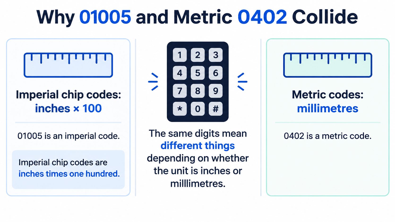
Then there's the word that starts the argument. In the imperial convention, a 01005 passive measures about 0.010 by 0.005 inch, or 0.25 by 0.125 mm. Much current assembly literature uses 01005 for the larger 0.4 by 0.2 mm part that formally carries the metric 0402 designation, as the IPC technical resource on package designation explains. Supplier bodies can also run from roughly 0.10 by 0.30 mm up to 0.20 by 0.40 mm depending on type and construction, so no code fixes an outline by itself.
<a id="what-a-swapped-code-corrupts-downstream"></a>
What a swapped code corrupts downstream
The error doesn't stay in the library. It travels through six downstream decisions: the land pattern, the feeder setup, the vision recognition model, the nozzle selection, the stencil aperture size and the solder-volume calculation. Each one gets configured from the code you typed, and each one is wrong together.
The failures that follow look unrelated to each other, which is what makes diagnosis slow. You get excessive pad overlap at one end and insufficient paste at the other. Then tombstoning, skew, open joints and inspection escapes appear across the same build, and the process engineer chases paste and profile while the underlying cause sits in the BOM.
Release rule: every passive line on the BOM carries the package code, the body length and width, the termination dimensions and the vendor's recommended land. A code without a drawing is a guess with a part number attached to it.
Read a datasheet 0402 written in millimetres as the miniature chip and a 0402 written in inches as the 1.0 mm by 0.5 mm part. If the datasheet doesn't state which system it uses, settle that question before the reel ships. Correcting a purchasing error costs far more than correcting a layout error of the same size.
<a id="land-patterns-that-fit-the-tiny-body"></a>
Land Patterns That Fit the Tiny Body
A 01005 gives you three sizes to keep separate: the physical body, the imperial-or-metric package code, and the copper land. The body typically measures about 0.4 mm by 0.2 mm. The code identifies which naming convention describes the part. The land has its own dimensions, set by the terminations and the solder fillets.
The copper works like a footprint cut for a particular shoe: the body can be the right size while the outline still loads the edges badly. A workable pattern gives each termination enough area to wet, leaves enough inner clearance to prevent bridging, and keeps the finished joint visible. Take pad length, pad width and gap from the drawing for the exact manufacturer part number (MPN). Another 01005 pattern can help you compare layouts, but its dimensions are not transferable.
| Feature | Typical figure or source | What to lock in CAD | |---|---|---| | Component body | Typically about 0.4 mm × 0.2 mm | Metric 0402, or a confirmed 01005 drawing | | Example capacitor pad | Manufacturer drawing for the selected MPN | Pad length and width per MPN | | Example land gap | Manufacturer drawing for the selected MPN | Inner gap on that capacitor pattern | | Alternate pad spacing | MPN-specific, not transferable | Confirm before reuse | | Resistor height | Typically about 0.1 mm | Keep the 3D body separate from the capacitor | | Capacitor height | Typically about 0.2 mm | Don't reuse the resistor footprint | | Mask, paste and courtyard | Vendor drawing, not a scaled 0201 | Mask clearance, aperture and courtyard |
<a id="six-fields-the-library-has-to-own"></a>
Six fields the library has to own
- Pad length: Set it from the termination length plus the heel and toe fillet you want. Body length only tells you how far the part extends over the copper.
- Pad width: Match it to the termination width with the side fillet in mind, because that fillet is where a bridge or an open shows up first.
- Inner gap: Take the dimension from the vendor land and confirm it against your paste-release window. A small shift can decide whether the deposits stay separate.
- Mask strategy and clearance: Choose non-solder-mask-defined or mask-defined before the fab files leave, and size the opening so ordinary registration drift doesn't change the wetted area at one end.
- Paste aperture: Express it as a share of the pad area and draw it on the stencil layer, never traced from the copper outline.
- Courtyard: Include placement tolerance, neighbour clearance, nozzle keep-out and a clear line of sight for the AOI camera.
<a id="why-halving-an-0201-land-fails"></a>
Why halving an 0201 land fails
Solder volume doesn't shrink in direct proportion to copper area. Reduce the land and the aperture together and the print can either crowd paste across the inner gap or leave too little volume at the toe. The first result bridges; the second reflows into a marginal joint. A DRC report sees legal shapes in both cases.
Spacing carries the same trade-off. The courtyard has to absorb placement error and leave the joint visible afterward. That constraint can limit density before the pad geometry does. A tighter pattern may free routing area, but the saving is poor value if it produces bridging, hides the fillet or leaves the camera nothing usable to inspect.
If you're rebuilding pad shapes from first principles rather than editing a vendor land, the basics of circuit board pad design still apply, compressed into a much smaller outline.
The library check takes an afternoon. One footprint per manufacturer part number, units confirmed as metric or imperial in the file name, the 3D height matched to resistor or capacitor rather than to the family, and the vendor drawing revision recorded on the footprint itself. Do that once and repeat builds stop inheriting the mistake.
A footprint that can't be inspected is a footprint that will ship with defects in it. Leave the camera something to see.
<a id="how-paste-placement-and-inspection-must-change"></a>
How Paste Placement and Inspection Must Change
A 01005 on a moving belt behaves like a grain of sand on a conveyor. It clings to tape, rides the nozzle longer than you expect, and blows off position when a puff of air crosses the feeder. Build the line so each station has exactly one job.
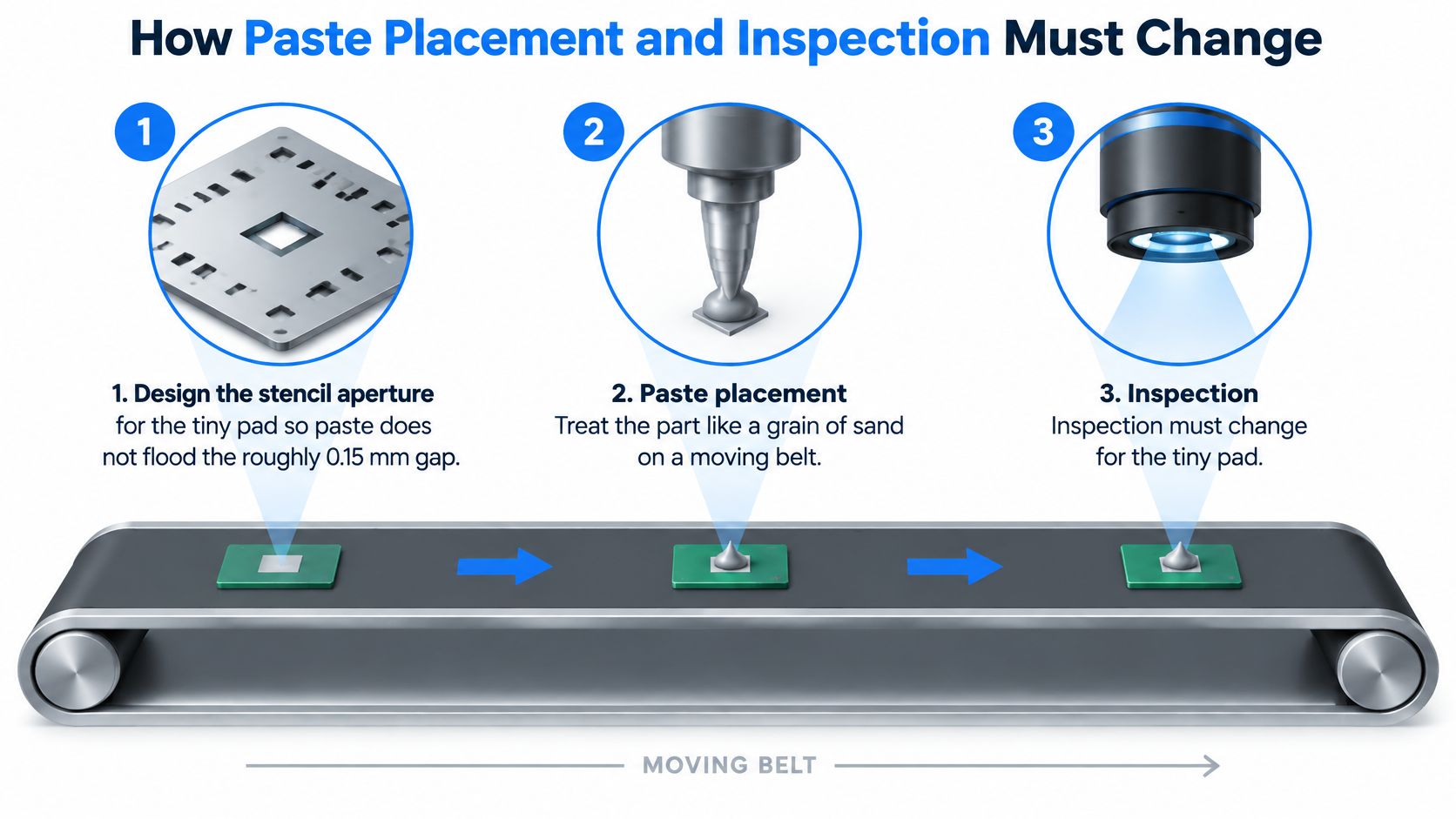
- Size the stencil aperture for the tiny pad, not for the copper. A thin foil in the 0.08 mm range with a nano coating releases paste at the low area ratios these apertures produce. A full copy of the copper outline floods the land gap and bridges; too aggressive a reduction starves the toe. One defect, one cause.
- Measure paste before anything is placed. Solder-paste inspection tells you volume, height, area and left-to-right balance while a bad print is still a board clean and a reprint. Skip it and the same defect reaches the finished assembly, where it can't be seen by eye.
- Match nozzle, feeder and vision to a part that weighs almost nothing. Pocket presentation, pickup height, vacuum release and tape type all decide whether the nozzle arrives at a centered part or a tilted one. Poor matching leads to missing components and side-placed parts.
- Cap placement force and Z-axis speed. This is not a smaller conventional chip that tolerates the same hit. Excess force squeezes paste out from under the terminations and can crack the body; too little travel leaves the part skating on the deposit.
- Reflow so both ends wet at the same moment. Unequal copper, a via in one pad or an asymmetric trace feeds one termination first, and the lighter end stands up. Balance the pad connections and the paste deposits before you touch the profile.
- Write an inspection recipe for this outline. A 2D camera can read a lifted termination as a good joint from directly above, so use angled or height-based AOI and keep X-ray for joints hidden under a body or beside a fine-pitch neighbour.
The print step deserves the most attention because it decides the rest. If you're setting aperture dimensions and stencil thickness from scratch, the principles of PCB stencil design apply at this scale with almost no margin for a rough transfer.
<iframe width="100%" style="aspect-ratio: 16 / 9;" src="https://www.youtube.com/embed/x3luNkPYbdY" frameborder="0" allow="autoplay; encrypted-media" allowfullscreen></iframe>A shop that advertises placement down to 0201 has not accepted this process, even when your Gerber fits its machine envelope. Ask what it runs for paste inspection, what stencil thickness it will use on your mixed panel, and how it verifies a joint it can't see. The answers tell you whether the quote is real.
<a id="when-to-use-01005-and-when-to-stay-on-0201"></a>
When to Use 01005 and When to Stay on 0201
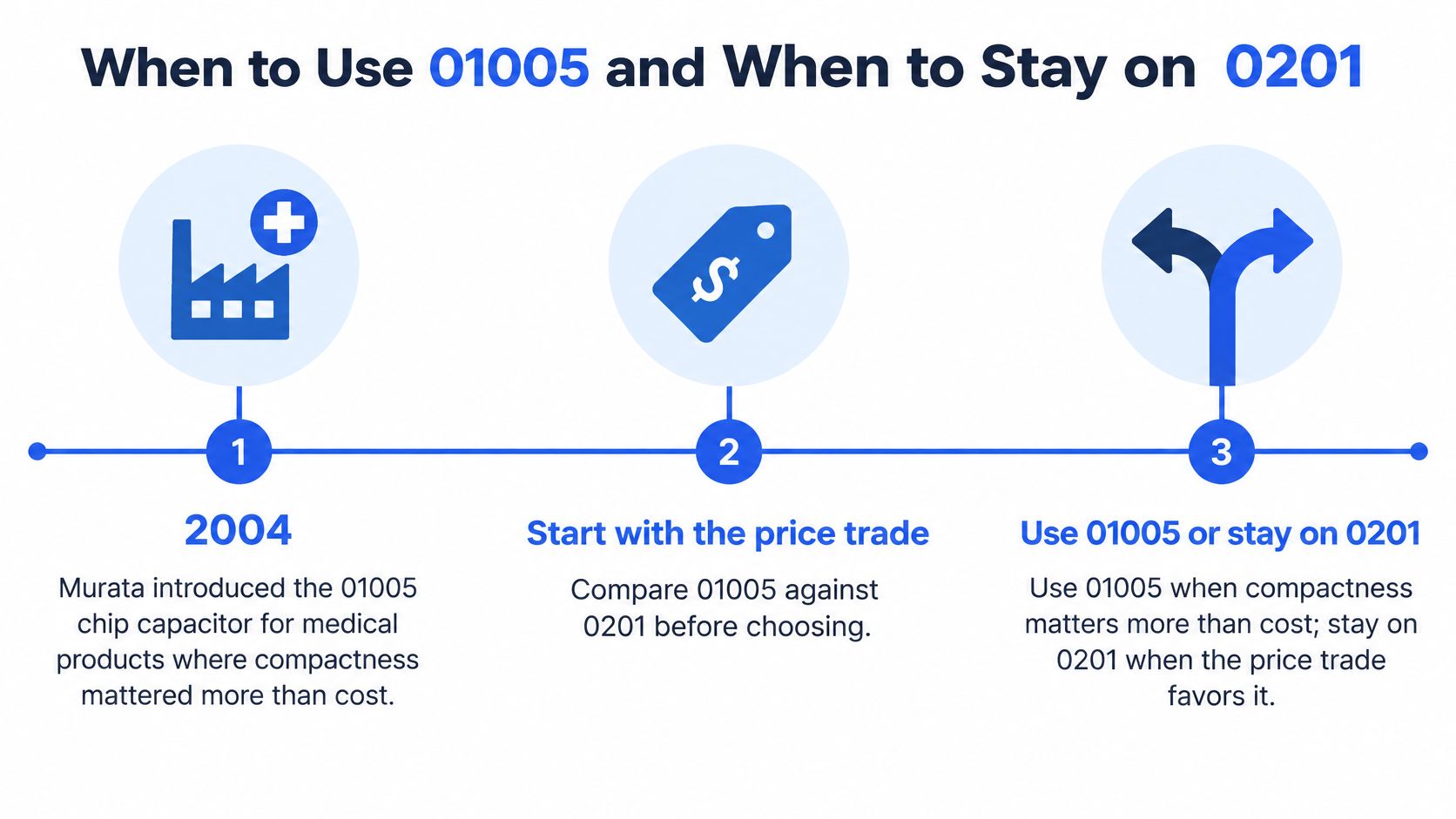
A manufacturing review of 01005 adoption records Murata introducing the 01005 chip capacitor in 2004, a 0.4 by 0.2 mm part presented as the smallest chip component of its day and aimed first at medical products where compactness outweighed cost, and it reports prices falling eightfold from that introduction level once production matured while the parts still sat about 12 times above the larger 0201 package, described in the comparison as 2.25 times larger. Production experience later carried the format into consumer electronics and demanding RF roles, including a 01005 high-Q multilayer ceramic capacitor Murata announced for cellular power-amplifier circuits. Density improved with each step. The unit-price gap stayed stubborn.
<a id="what-the-area-saving-has-to-buy"></a>
What the area saving has to buy
The layout arithmetic is still the strongest argument for the smaller part. Per assembly reporting on 01005 process limits, cutting spacing from 0.2 mm to 0.1 mm saves up to 35 percent of area, and moving from 0402 to 01005 at 150 µm spacing saves approximately 74 percent. The same account notes limited available values, relatively high component cost and difficult production processes, and warns that placement force above roughly 2 N may damage the component.
Those numbers set the negotiation, and they also expose what is really changing. Choosing this package shrinks three sizes at once: the ceramic body, the code printed on the reel, and the copper land your line prints onto. The first two cost nothing to shrink. The third is where the yield penalty lives, because the land is what paste, placement and inspection all have to work with.
<a id="where-each-package-wins"></a>
Where each package wins
| Situation | What you gain | Better package choice | |---|---|---| | Area is the constraint | Up to about 35 percent if spacing goes from 0.2 mm to 0.1 mm | 01005 if the value exists | | Replacing 0402 at 150 µm spacing | About 74 percent area saved | 01005 on a capable line | | Dense RF, phone, wearable or IoT | Height and matching-network area | 01005 | | Broad values or easier sourcing | Wider catalog and lower part price | 0201 or 0402 | | Weak placement or inspection | A wider force margin and joints a camera can see | 0201 or 0402 | | Rework and field service matter | Larger joints that can be touched up | 0201 or 0402 |
A "capable line" is a shop that lists 01005 inside its assembly envelope and can show the inspection behind it, the way a turnkey PCB assembly service states its smallest chip size alongside its test steps. If your assembler cannot, the 01005 column in this table is empty for your board.
A wearable matching network justifies the penalty: the value probably exists in the small size, the area is unavailable, and the board will never see a soldering iron after it leaves the line. A serviceable industrial controller usually can't make the same case, because a field return that needs a single passive replaced becomes a scrapped assembly.
The question to bring to schematic review: what measured area, height or RF benefit offsets the sourcing, placement and inspection cost of this outline on this board?
If the answer is "it's the smallest size available", lay the board out at 0201 first and measure what 01005 would recover. The freed area is often smaller than the body ratio suggests, because spacing rules, routing and via placement hit their limit before the package does. The body saves the square millimetres. The land and the spacing decide whether you get to keep them.
<a id="confirm-the-footprint-before-you-build"></a>
Confirm the Footprint Before You Build
Three checks before the files leave, in order. Match the datasheet body to the millimetre table and reject any library part whose 0402 turns out to be imperial. Confirm pad size, inner gap, mask clearance and courtyard against the manufacturer drawing, with separate footprints for the resistor and the capacitor. Get the assembler's confirmation in writing that it places 01005 by intent on this panel, which file set it accepts, and whether its AOI and X-ray recipes cover joints this small.
Only then release the Gerber, BOM and pick-and-place files. On our side, turnkey assembly handles the 01005 component size through BGA and QFN packages with a 0.35 mm minimum pitch, and the flow includes AOI, X-ray and functional test, so the design question and the verification question get answered by the same team.
The goal is a footprint you can defend with a drawing, not a board where every passive shrank because the smallest option existed. Send the confirmed land pattern with the BOM and the package code stops being a coin flip.
Lianyuhong Technology Co.,Ltd assembles from the 01005 component size up through fine-pitch BGA and QFN, with SPI, AOI, X-ray and functional test inside the same build, so the artwork you approve is the artwork that gets verified. Send your Gerber or ODB++, BOM and pick-and-place files and our engineers will review the package codes, land patterns and stencil plan before anything is cut. Visit Lianyuhong Technology Co.,Ltd to start that review.