
A solder-paste stencil is the cheapest item in an SMT build and the one that decides whether the rest of the line works. Technavio's 2024 forecast put global PCB solder-paste stencil growth at USD 213.1 million between 2023 and 2028, a 5% compound annual growth rate (Research and Markets listing of the forecast). Most of that pressure comes from boards that mix 01005 passives, fine-pitch QFNs and power pads on the same panel.
The 0.66 area ratio gets quoted as if it were a guarantee. It isn't one. A design can clear it on every aperture and still come back from the printer with half-empty fine-pitch pads, because the ratio describes how paste releases from an aperture wall, not the volume that lands on the pad.
Where re-orders come from is rarely the printer. They come from a foil chosen to suit the biggest pad on the board, from spacing never checked on a dense connector, and from a paste layer sent to the shop at pad size with the reduction left to whoever is cutting. All three are geometry decisions made in CAD, weeks before paste is on the board.
Table of Contents
- Aperture Rules That Set Every Opening Size
- Foil Thickness by Component Mix
- How to Calculate Every Aperture Before Drawing
- Thermal Pads and Mixed-Technology Boards
- Finishes and Files for the Stencil Shop
- Confirm the Stencil Design With SPI Data Before Release
<a id="aperture-rules-that-set-every-opening-size"></a>
Aperture Rules That Set Every Opening Size
The 0.66 area ratio is a starting threshold, not proof that an aperture will print well. It describes the opening area relative to the area of its walls, which affects how readily paste releases. It does not confirm that the deposited volume will meet the joint's needs. Treat it as a screening check, then verify print results with SPI data.
<a id="why-small-openings-fail-first"></a>
Why Small Openings Fail First
As an aperture shrinks, its walls take up a larger share of the opening. Paste can cling to those walls during stencil separation instead of transferring cleanly to the pad. A small opening may therefore produce an incomplete deposit even when its design clears the area-ratio threshold.
For fine-pitch leads, set aperture width with the lead geometry and paste volume in mind. Reducing openings on larger-pitch components can help control excess paste and bridging, but an aggressive reduction can also leave joints short of solder. The right geometry depends on the component and the print results, not on a single ratio applied across the board.
Aperture rules for SMT stencil design
| Rule | Target | How to calculate | Basis | |---|---|---|---| | Area ratio | 0.66 or higher as a starting threshold | Aperture opening area divided by aperture wall area | Indicates release potential; confirm performance with SPI | | Aspect ratio | Greater than 1.5 as a starting point | Aperture width divided by foil thickness | A screening check for paste release | | Fine-pitch aperture width | Set for the lead geometry and required paste volume | Compare opening width with lead pitch and pad dimensions | Balance release against bridging risk | | Larger-pitch apertures | Consider reducing where excess paste risks bridging | Compare the opening with the pad and joint requirements | Avoid excessive deposits without starving the joint | | Adjacent aperture spacing | Keep enough separation for reliable printing | Measure the gap between neighbouring openings | Tight spacing can increase bridging risk | | Paste transfer | Confirm with SPI data | Compare deposited paste with the intended deposit | Area ratio alone does not confirm print performance |
Check each aperture class, not just the smallest opening. If a fine-pitch aperture fails, changing the whole foil may reduce paste volume on larger pads as well. On boards that combine 01005 apertures with large thermal pads, assess those needs separately before choosing one foil thickness and aperture strategy for the entire stencil.
Practical rule: Treat the marginal aperture as the problem to solve. Change the foil only when the same limitation affects a broader group of openings.
<a id="foil-thickness-by-component-mix"></a>
Foil Thickness by Component Mix
A stencil that prints both 01005 pads and large thermal pads has competing paste-volume needs. Set foil thickness around the smallest openings first, then check whether larger pads still receive an adequate deposit. If the large pads drive the choice, fine-pitch components may suffer incomplete or inconsistent paste release.
Foil thickness by smallest aperture
| Component | Smallest aperture | Foil thickness | Area ratio at that size | |---|---|---|---| | 01005 and 0201 passives | 0.20 mm square | 3 mil (75 µm) | 0.67 | | 0.4 mm pitch BGA and QFN | 0.20 mm square | 3 mil (75 µm) | 0.67 | | 0.5 mm pitch QFP and QFN | 0.25 mm square | 4 mil (100 µm) | 0.63 | | 0.65 mm pitch and connectors | 0.35 mm circle | 5 mil (125 µm) | 0.70, passes |
Three mil, about 75 µm, is a common starting point for 01005, 0201 and very small CSP apertures. A 0.20 mm square in this foil gives an area ratio of about 0.67. For 0.65 mm pitch parts and connectors, 5 mil foil gives a 0.70 area ratio at a 0.35 mm circular opening. Treat both values as design checks, then confirm paste transfer with SPI data.
<a id="the-4-mil-trap"></a>
The 4 mil trap
Four mil can look like a reasonable compromise, but it reduces release margin for small apertures. A 0.20 mm square in 4 mil foil has an area ratio of about 0.50, while a 0.25 mm square has about 0.63. Both fall below the 0.66 starting threshold, so verify these aperture classes with SPI rather than assuming they will print reliably.
Foil thickness affects every opening. Once selected for the smallest apertures, size the remaining openings to suit that thickness. If 01005 apertures need thin foil while thermal pads need more paste, consider a stepped or hybrid stencil rather than compromising on one thickness across the board. Confirm the choice against SPI results, since the 0.66 threshold is a starting point, not a guarantee of consistent transfer.
<a id="how-to-calculate-every-aperture-before-drawing"></a>
How to Calculate Every Aperture Before Drawing
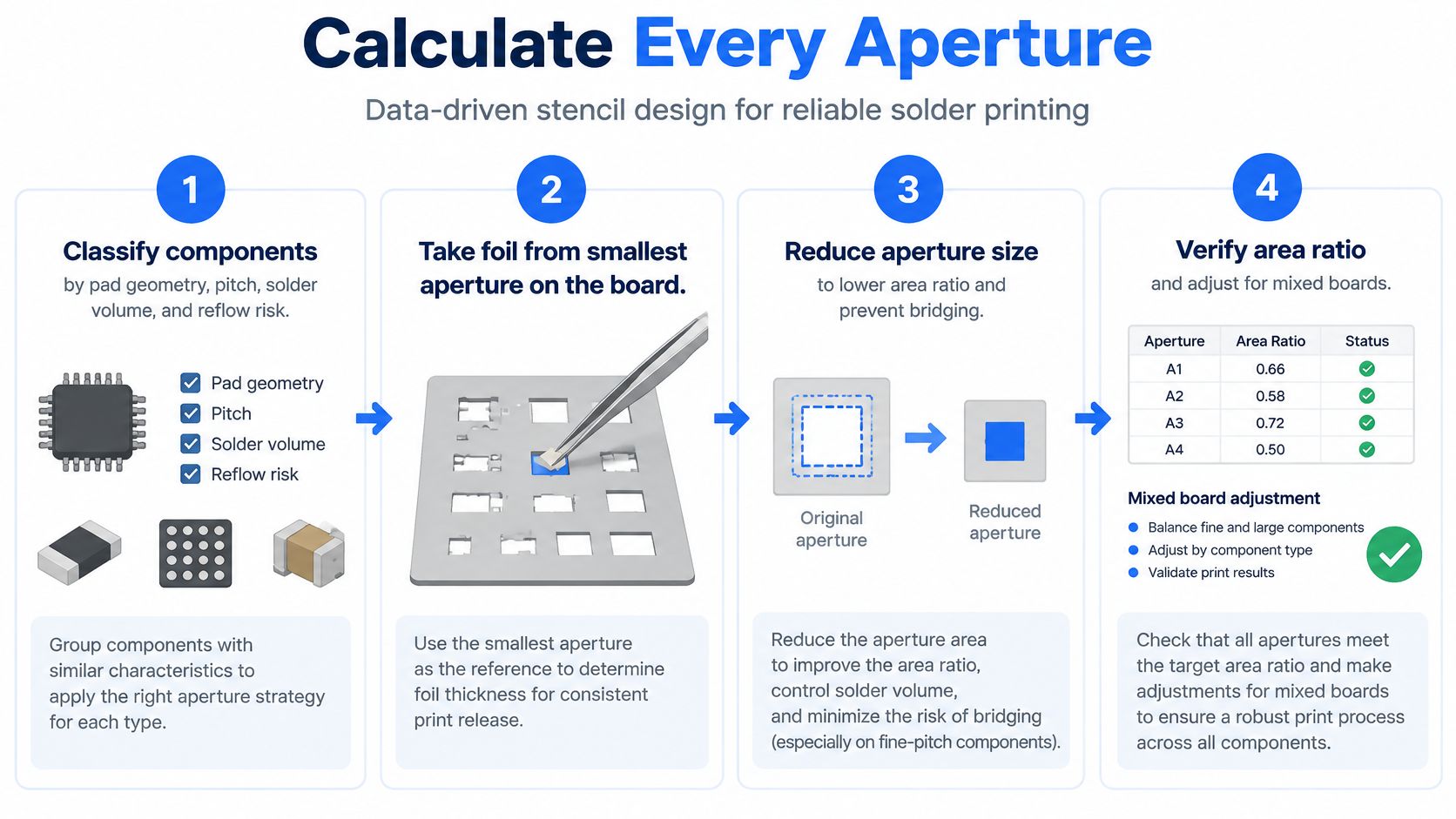
The calculation sequence matters because each decision limits the next. The EPC application note on PQFN and GaN stencil design offers related guidance for assemblies with thermal pads.
- Classify each component by pad geometry, pitch, solder-volume needs, and reflow risk. A 01005 aperture and a QFN thermal pad impose different paste-deposition demands.
- Set foil thickness from the smallest aperture. It has the least release margin and is the first opening to check against the foil.
- Calculate both ratios for each aperture. Aspect ratio is aperture width divided by foil thickness; a common starting minimum is above 1.5. Area ratio is opening area divided by the area of its walls; 0.66 is a starting threshold, not a guarantee of reliable release.
- Check spacing between openings. A common guideline is to keep the gap at least 15 µm greater than the foil thickness. At 3 mil foil, that means a 90 µm gap.
- Check paste deposits against SPI data. Passing the ratios does not confirm that a joint receives the required solder volume. Treat 0.66 as a threshold to verify against measured deposits, not as proof that every aperture will print well.
For a square aperture, area ratio simplifies to width divided by four times the foil thickness. The four aperture walls each have an area equal to width multiplied by foil thickness. For a circular aperture, use the diameter in the same formula.
A 0.20 mm square in 3 mil foil gives 0.20 ÷ 0.30, or 0.67. In 4 mil foil, the same opening gives 0.50.
<a id="one-board-two-apertures"></a>
One board, two apertures
Consider a panel with a 0.4 mm pitch BGA using 0.20 mm square apertures and a 0.5 mm pitch QFP using 0.25 mm squares. The BGA sets the foil at 3 mil, giving an area ratio of 0.67. The QFP reaches 0.83 at that thickness, so both component groups can use one foil, subject to SPI confirmation.
If a large thermal pad on the same board receives too little paste, changing the foil also changes release conditions for the BGA apertures. Check the thermal-pad opening pattern before changing thickness. Common calculation errors include selecting foil thickness from the largest pad, using the square-aperture formula for round openings, and overlooking tight spacing between connector apertures.
<a id="thermal-pads-and-mixed-technology-boards"></a>
Thermal Pads and Mixed-Technology Boards
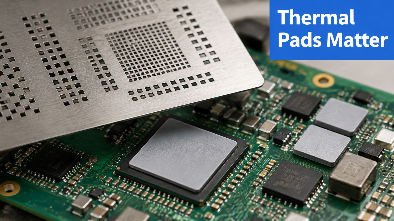
Reducing every aperture on a dense board feels cautious. It isn't. Shrinking openings cuts bridging and solder balls on fine-pitch devices, but it also lowers area ratio and makes release more variable on openings that were already marginal, which is why aggressive reduction is not automatically the safer direction on a board that mixes pad scales (01005 land pattern and stencil guidance).
The hard case is a board with 01005 passives at one end and a large QFN thermal pad at the other. Standard advice, choose the foil from the smallest aperture and then check whether the larger packages still get enough paste, tells you to look but not what to do when the answer is no. The section below is that decision, made component group by component group.
Strategies for boards that mix aperture sizes
| Strategy | Use when | Main trade-off | |---|---|---| | Single foil stencil | Every aperture passes area ratio at one thickness | Only works for a uniform component mix | | Stepped stencil | Fine-pitch and large pads need different paste volumes | Higher fabrication cost and more setup | | Local aperture reduction | A few oversized pads hold too much paste | Lower volume may weaken some joints | | Window-pane thermal pad | QFN or BGA thermal pads trap gas during reflow | Less paste, so X-ray checks are required | | Separate print passes | Two paste types or heights on one board | Extra process steps and alignment risk |
<a id="segmentation-is-a-trial-variable-not-a-recipe"></a>
Segmentation is a trial variable, not a recipe
A full 1:1 opening on a thermal pad maximizes paste volume and, with it, the gas trapped under the package during reflow. Window-pane or segmented patterns break the deposit into smaller areas so volatiles have escape paths, and that is the usual starting point for QFN and BGA thermal pads (stencil aperture geometry and area ratio guidance).
The trap is treating segmentation as a fixed pattern. Cut too much away and the thermal and electrical connection thins out, and print-to-print variability climbs. Print two or three segmentation variants on the same coupon, X-ray each one, and keep the pattern with the lowest voiding that still delivers the joint volume the thermal design needs. Repeat the trial whenever the alloy or a vacuum reflow step changes, because both shift voiding behaviour.
Mixed-technology panels also carry through-hole parts alongside the SMT pads, which changes print and place order and sometimes the support tooling (surface mount versus through hole assembly).
<a id="paste-and-foil-move-the-same-needle"></a>
Paste and foil move the same needle
Geometry is only half the release story. In one IPC study, Type 4 paste released better than Type 3 with confidence above 95%, and 3 mil foil released better than 4 mil foil at the same confidence level, while square apertures averaged better release than circular ones without reaching statistical significance (IPC stencil printing study). The same work reported a 5 mil foil at area ratio 0.60 averaging 85 to 92% transfer efficiency with standard deviation under 10%, against 65% average transfer for a 230 µm square pattern.
Two numbers that far apart, from apertures in the same ratio neighbourhood, explain why the ratio is a starting threshold. Paste alloy, particle distribution, wall finish, board support and printer settings decide the rest.
<a id="finishes-and-files-for-the-stencil-shop"></a>
Finishes and Files for the Stencil Shop
Finish is a release decision, not a cosmetic one. Untreated laser-cut stainless steel is the baseline: it works, the aperture walls come out slightly rougher, and it suits parts at 0.5 mm pitch and larger where there's release margin to spare. Nano coating lowers the surface energy on the walls so paste stops sticking, which buys margin on fine-pitch and small apertures. Electropolish smooths the walls after cutting and suits dense mixed boards carrying 01005 parts, where every bit of wall adhesion counts against you.
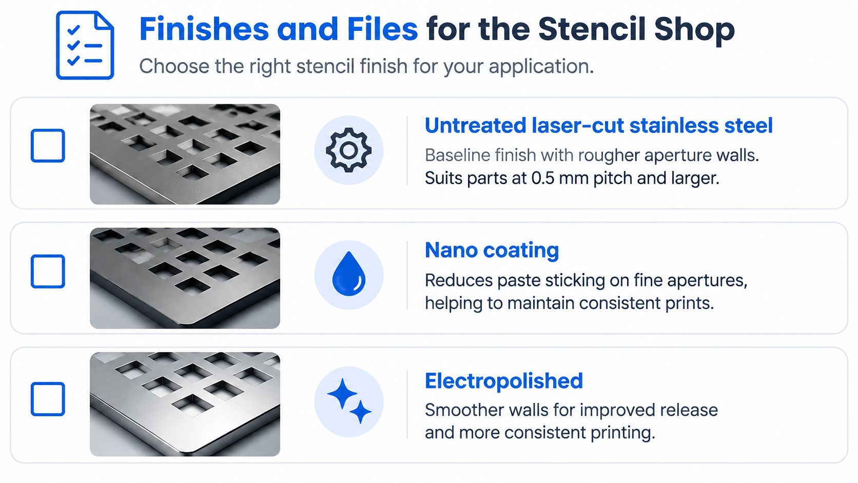
We cut stencils from laser-cut 304 HTA stainless steel in 0.08 mm to 0.3 mm thickness with nano coating or electropolishing as an option, which covers the pitch range from 01005 through coarse connectors in one material family.
<a id="the-file-set-that-avoids-a-second-order"></a>
The file set that avoids a second order
- A paste-layer Gerber, or ODB++ and native CAD where the shop accepts them, with apertures drawn at the final reduced size rather than at pad size.
- A stated foil thickness that matches the one the area ratio table produced, not the default the shop stocks.
- Frame and panel dimensions, with datum and fiducial positions matching the board so the stencil registers on the printer.
- An aperture schedule listing every locally reduced, windowed or stepped aperture and the reason for it.
- Finish and tension requirements, since nano coating and electropolish change lead time and cost differently.
The mistake behind most re-orders: sending pad-size data and letting the shop infer the reduction. The stencil that arrives reflects a different design from the one that was reviewed, and nobody discovers it until the first print.
Annotate every modified aperture on the drawing. A shop reviewing an unexplained reduction can't tell an intended change from a copy error, and it will cut what the file says either way. Whoever is doing the cutting only sees the file, so pick a PCB stencil manufacturer that checks the aperture schedule against the paste layer before the foil goes on the laser. When the design isn't in Gerber, send ODB++, Altium, Eagle or KiCad files instead, which we accept as contact-request attachments up to 20 MB.
<a id="confirm-the-stencil-design-with-spi-data-before-release"></a>
Confirm the Stencil Design With SPI Data Before Release
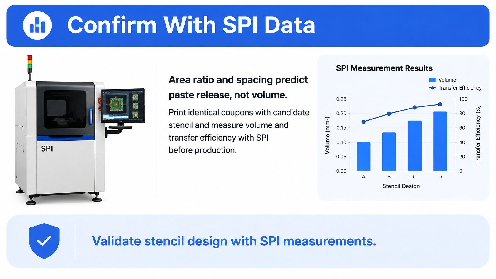
Area ratio and spacing predict whether paste releases from a wall. They don't predict how much lands on each pad, and that gap is where a design that passed every calculation still ships bad boards. A stencil shop cuts what you send, so the confirmation step belongs to the team that owns the aperture table.
Print identical coupons with the candidate stencil and measure volume and height for each pad class separately: 01005, fine-pitch QFP, BGA, thermal pad. Comparing measured volume against the volume the aperture geometry implies is the whole test, and it separates a geometry problem from a printer problem in one run.
<a id="set-the-limits-before-the-first-print"></a>
Set the limits before the first print
Write the acceptance criteria down before the coupon goes on the printer, because a limit invented after you've seen the data isn't a limit.
- Mean volume band around target for each pad class, so an over-printing class can't hide behind a passing average across the panel.
- A standard deviation ceiling for critical pads, since a stable mean with a wide spread still produces opens at the low end.
- An outlier rule, defining how many deposits outside the band trigger an aperture change rather than a printer tweak.
Then read the distribution shape, not just the average. A tail of low deposits confined to the 01005 row is a release problem in that aperture class. Raising print pressure or slowing squeegee speed to chase it usually pushes paste onto the stencil face and creates bridging elsewhere, while the tail stays.
<a id="the-release-sequence"></a>
The release sequence
- Lock the aperture table, with a written reason against every modified aperture.
- Print the coupon with the candidate stencil on the production printer, not a lab unit.
- Measure with SPI and compare against the pre-agreed limits.
- Adjust only the failing aperture classes, leaving passing ones untouched.
- Release the file set using the checklist above, with the foil thickness and finish called out.
The pitfalls worth naming are approving a stencil on a single panel position instead of across the full panel, using the wrong paste type on marginal apertures, and letting board support and foil cleanliness slide during the trial, which makes the data look worse than the design.
Release gate: if the coupon's volume distribution doesn't clear the limits, the design isn't ready, no matter how clean the area ratio table looks.
For a prototype build where the first panel doubles as the qualification vehicle, prototype PCB supplier turnaround decides how many revision cycles you can afford, and two or three SPI-guided cycles close a mixed-technology stencil far faster than six rounds of building and reflowing whole boards.
Lianyuhong Technology Co.,Ltd cuts SMT stencils from 304 HTA stainless steel in 0.08 mm to 0.3 mm thickness with nano or electropolish finishes, and our assembly lines run the SPI, AOI and X-ray checks that confirm a design before it goes to production. If you're releasing a board that mixes 01005 passives with fine-pitch BGAs or large thermal pads, send us the paste layer along with your Gerber, ODB++ or native CAD files and we'll review the aperture set against your component mix before anything is cut. Visit Lianyuhong Technology Co.,Ltd to start a stencil order or a stencil-plus-assembly quote.