
More than 96 percent of the failures in a NASA thermal-cycling program on a CGA, LGA and HDI assembly were pad cratering and pad lift, found by dye-and-pry inspection after the boards left the chamber (NASA NEPP BGA guidelines). Not solder-joint cracks. Not ball opens. The laminate under the copper, and the bond holding the copper to it, did the failing.
That one result reorganizes how circuit board pads should be chosen. A pad isn't the passive rectangle a footprint library hands you. It's the mechanical anchor between component and board, the wettable surface for the joint, a thermal path into the stack, and the place where expansion mismatch gets squeezed into a few square millimeters of resin and foil.
Every decision about it, its type, its size, its mask definition, the via you drop inside it, trades one kind of reliability for another.
Table of Contents
- Circuit Board Pad Types at a Glance
- Pad Sizes and the 0.05 mm Design Grid
- Fine-Pitch Pads, Solder Mask and Stencil Apertures
- Pad Reliability Numbers and Failure Modes
- Choosing Between SMD and NSMD Pad Definitions
- When Via-in-Pad Is Safe to Use
- Confirm Your Pad Design Before Release
<a id="circuit-board-pad-types-at-a-glance"></a>
Circuit Board Pad Types at a Glance
Six pad types cover nearly every part you'll place. Here's the map before the detail.
| Pad type | Location | Main purpose | Typical use | |---|---|---|---| | SMD pad | Outer layer, surface | Solder surface-mount terminals | Chips, resistors, QFP, BGA, QFN | | Through-hole pad (annular ring) | Drilled hole, all layers | Hold leaded terminals mechanically and electrically | Connectors, electrolytic capacitors | | Via-in-pad | Via placed inside a pad | Route under a component | Fine-pitch BGA with filled and capped vias | | Thermal pad | Under QFN or power IC | Conduct heat into internal planes | Power ICs, LED drivers | | Test pad | Outer layer, unmasked | Give probe access for test | Flying probe and in-circuit test points | | Castellated edge pad | Board edge | Mount a module onto a carrier board | Wi-Fi and Bluetooth modules |
A pad is a landing strip. It's sized and placed so the component's contact touches down on exactly the right copper, with enough margin for a solder fillet and enough clearance that the neighboring resist doesn't crowd it.
SMD pads do nothing but solder, which is why they're the easiest to get wrong through carelessness rather than analysis. Through-hole pads carry a second job: the annular ring has to survive insertion force and rework heat as well as make the connection. Via-in-pad solves a routing problem by moving a hole into the landing zone, and it inherits every process risk that comes with that. Thermal pads exist to dump heat into internal planes, so their via array is part of their electrical function, not an afterthought.
The same copper shape can serve different jobs depending on mask and paste. A rectangular land with resist opening larger than the copper behaves as an NSMD pad; the identical land with resist overlapping the edge behaves as an SMD pad. Same geometry, different mechanics, different failure mode.
<a id="how-to-read-the-pad-type-off-a-datasheet"></a>
How to Read the Pad Type Off a Datasheet
- Surface-mount or leaded? This settles SMD versus through-hole in one glance at the mechanical drawing.
- Exposed thermal pad? If the package outline shows a central pad under the body, you owe it a via array and a paste strategy.
- Hidden joints? BGA and QFN terminals sit out of sight, so the pad design and the inspection method have to be decided together.
- Module on a carrier? Castellated half-holes at the edge mean the pad is a solderable wall, not a flat land.
By the end of a footprint review you should be able to name the pad type for every part on the board without opening the library a second time.
<a id="pad-sizes-and-the-005-mm-design-grid"></a>
Pad Sizes and the 0.05 mm Design Grid
Pad dimensions sit on a grid that changed units mid-career for many readers. From the 1960s through the 1980s, board features were laid out on a 0.001 inch grid, one mil, in symmetrical and evenly balanced geometry. In 1988 international standards organizations began coordinating a move to metric, and IPC proposed 0.05 mm as the base value of a universal design grid. Through the 1990s component makers and JEDEC converted package and land-pattern data from inch dimensions to metric, and by 2001 JEDEC and most suppliers had largely adopted metric measurements, as IPC's technical paper on the metric design grid records.
That 0.05 mm step now governs pad sizes, drilled holes, plane antipads, thermal reliefs, line widths, snap grids and polarity markers. It's why fine-pitch, BGA, HDI and microvia layouts are routinely specified in millimeters even when the library behind them still speaks in mils.
The practical consequence lands on a single board with a mixed vocabulary. A pad has to satisfy the component package data, the stencil aperture, the solder-mask clearance and the fabricator's capability at the same time, and those four inputs rarely arrive in the same unit. A metric land pattern keyed into a mil field is wrong by a factor of 25.4, which is the sort of mistake that survives DRC and dies at first article.
<a id="the-sizing-order-that-prevents-rework"></a>
The Sizing Order That Prevents Rework
- Start from the datasheet land pattern. The supplier's recommendation already accounts for terminal shape and stand-off. Libraries go stale; datasheet revisions don't.
- Check for the fillet, not just the fit. Pad width must leave copper beyond the terminal so solder can form a concave fillet at the side and heel. A pad exactly the width of the terminal looks tidy and solders badly.
- Hold the annular ring above the fabricator's minimum. Through-hole pad diameter is the drilled hole plus twice the annular ring. Ask for the shop's floor rather than assuming a number from an older project.
- Add mask clearance deliberately. Too little and resist creeps onto copper that should wet; too much and you expose neighboring traces and invite bridging. Set it per component class, not once per board.
- Confirm the unit at every handoff. Library, schematic, fab drawing and assembly drawing each get their own chance to change the interpretation.
Before fabrication files go out: open the datasheet drawing beside the library land pattern, export a dimension report from CAD, and confirm whether the library stores millimetres or mils. Ten minutes here beats a respin.
<a id="fine-pitch-pads-solder-mask-and-stencil-apertures"></a>
Fine-Pitch Pads, Solder Mask and Stencil Apertures
At 0201 and 01005 sizes, small changes to copper, mask openings or paste volume can alter the joint. Design these features together, because each one affects the process window for the other two.
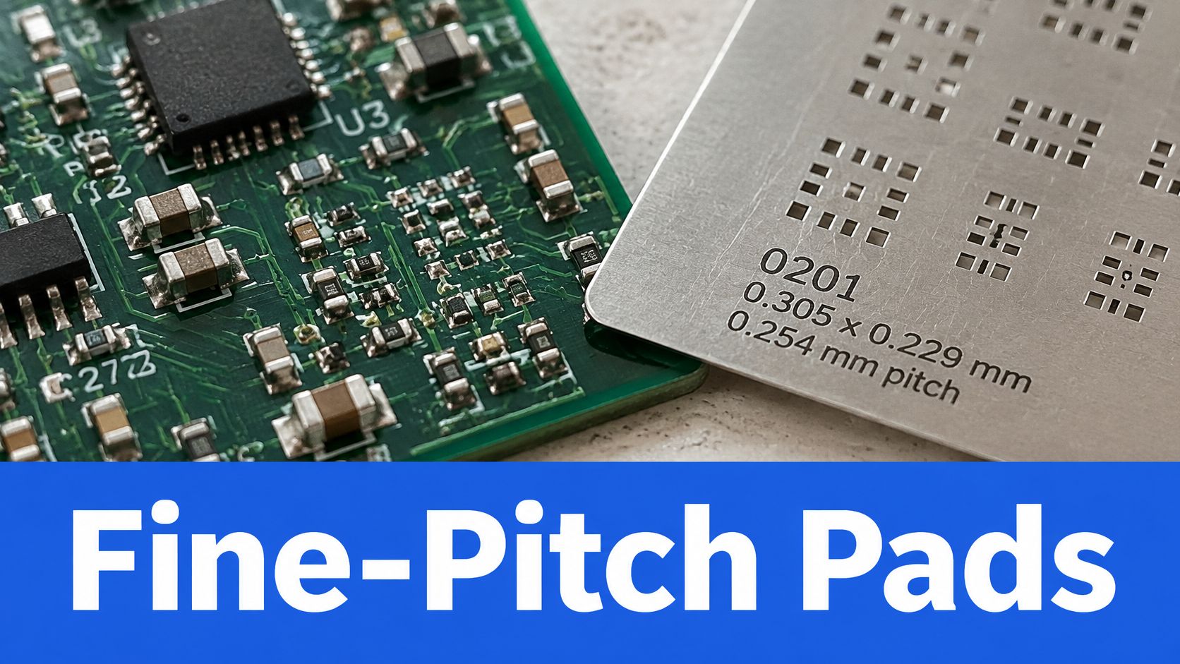
An IPC evaluation of 0201 components compared two land layouts, showing how geometry can affect reflow behavior and defect risk for the same component.
| Layout | Land spacing | Land size | What was studied | |---|---|---|---| | Layout A | 0.254 mm | 0.305 mm × 0.229 mm | Reflow behavior and defect risk with wider spacing | | Layout B | 0.229 mm | 0.381 mm × 0.305 mm | Reflow behavior and defect risk with tighter spacing and larger lands |
Neither layout is universally correct. Layout B combines tighter spacing with larger lands, changing the risk of bridging or component movement. Layout A provides more spacing but changes the available copper for wetting. Choose dimensions against the assembly process, not as a drafting convention.
<a id="three-controls-that-have-to-move-together"></a>
Three Controls That Have to Move Together
Copper geometry sets the joint's available solder area. Solder-mask definition controls the exposed copper and the position of the mask edge. Stencil aperture controls paste delivery. If one changes, check the other two before releasing the design.
For very small components, NSMD pads can accommodate some solder-mask registration variation because the mask opening extends beyond the copper land. Apertures must still be designed for the component and process, with attention to paste deposits, bridging and movement during reflow. Avoid scaling apertures by a blanket area ratio alone.
For 01005 assemblies, elliptical solder-mask-defined pads are one geometry to consider. Their suitability depends on the complete process window, including PCB and stencil tolerances, cleanliness and placement accuracy. A pad shape cannot compensate for a process that cannot hold those controls.
<a id="the-verification-path-that-catches-what-dimensions-cant"></a>
The Verification Path That Catches What Dimensions Can't
MicroBGA joints are hidden from direct visual inspection, so verification needs to cover both printing and the completed assembly. Release padstacks alongside paste apertures and mask rules. Use SPI to assess paste volume and registration after printing, AOI after placement, and X-ray or cross-section when joints are inaccessible.
Stencil cut and finish affect paste release. The guide to PCB stencil design explains the design choices involved.
Rule: A pad change requires a matching review of paste and mask settings. Keep the padstack, aperture and mask rule under the same design revision.
<a id="pad-reliability-numbers-and-failure-modes"></a>
Pad Reliability Numbers and Failure Modes
Four stress sources decide whether a pad survives its service life: thermal cycling, expansion mismatch between package and board, board bending, and the strength of the copper-to-laminate interface. Wetting behavior tells you almost nothing about any of them.
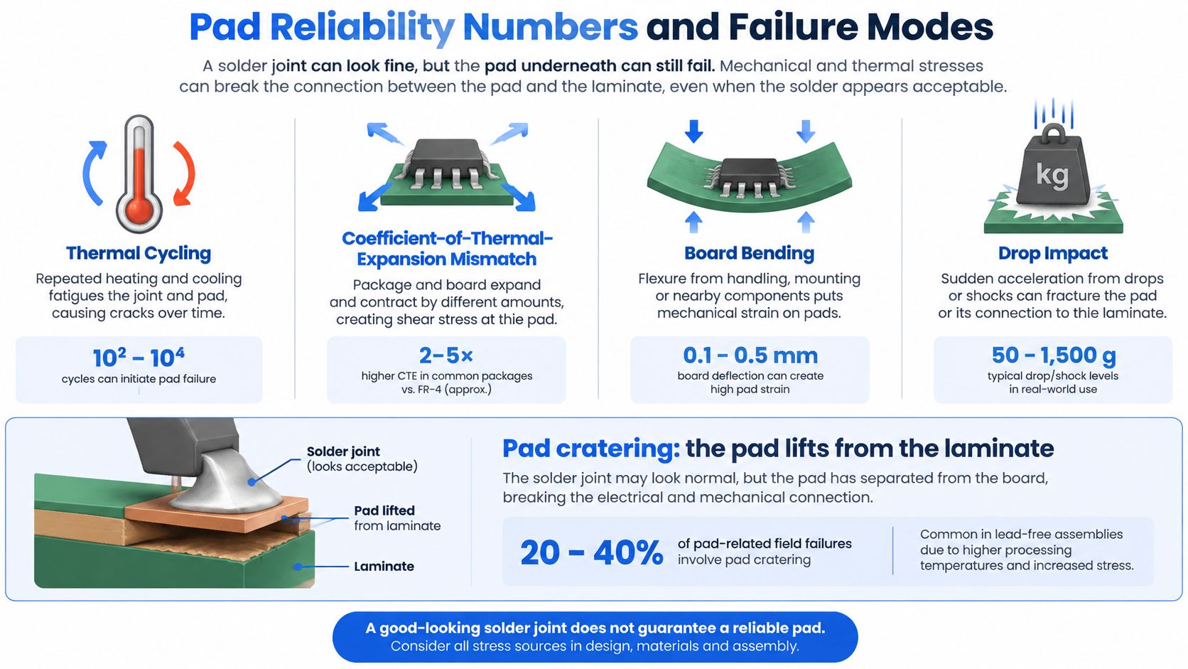
NASA's BGA guidelines put numbers on the outcome.
| Metric | Value | Context | |---|---|---| | Typical BGA solder-joint life | About 100 to 6,000 thermal cycles | Temperature excursions from -55 °C to 100 °C | | Effect of larger temperature swings | Shorter life | General NASA guidance | | Pad lifting in CGA, LGA and HDI test | 38 of 1,034 sites (about 3.7%) | After thermal cycling | | Failures from pad cratering and pad lift | More than 96% of observed failures | Dye-and-pry testing after thermal cycling |
Look at the pad-lift count against the joint-life range. A joint that survives thousands of cycles can still be sitting on copper that has already separated from the resin beneath it, and no amount of electrical test will tell you.
<a id="two-failure-modes-worth-naming"></a>
Two Failure Modes Worth Naming
Pad lift is copper peeling away from the laminate. The joint may be intact, the ball may be round, and the net may still read continuity, but the mechanical anchor is gone and the next thermal excursion finishes the job.
Pad cratering is the laminate cracking under the pad. It starts as a resin fracture beneath the copper, often at a corner where the stress concentrates, and propagates until the land separates. Dye-and-pry is how you find it, because it's invisible from above.
High-density packages concentrate both. Small pads mean less area to distribute stress. Rigid lead-free joints pass more strain into the land. Thin dielectric structures flex more under the same load, and repeated temperature change ratchets the interface until it gives.
<a id="the-levers-that-actually-move-the-number"></a>
The Levers That Actually Move the Number
- Copper geometry: larger lands and rounded corners spread stress instead of concentrating it at a sharp edge.
- Laminate selection: the resin system under the pad is the failing material in most cratering cases.
- Expansion mismatch: package and board move differently, and the pad absorbs the difference.
- Warpage control: a board that bows during reflow preloads the joints before service even starts.
- Temperature profile: ramp and soak shape the residual stress the assembly carries out of the oven.
- Inspection of hidden joints: if you can't see it, plan the X-ray or cross-section before the build, not after a field return.
If you want to watch cratering happen rather than read about it, this walkthrough is worth ten minutes before your next BGA review.
<iframe width="100%" style="aspect-ratio: 16 / 9;" src="https://www.youtube.com/embed/TLqeu9Y6k_E" frameborder="0" allow="autoplay; encrypted-media" allowfullscreen></iframe>A reliability target needs cycle counts and failure counts attached to it, plus the inspection method that produced them. A single pass result on one assembly tells you that assembly survived one test, which is a different claim entirely. For the assembly-side controls that support those numbers, see our notes on BGA PCB assembly.
<a id="choosing-between-smd-and-nsmd-pad-definitions"></a>
Choosing Between SMD and NSMD Pad Definitions
Ask a room of layout engineers whether to use SMD or NSMD and you'll get one answer: NSMD, every time, because it wets better. That answer is half right, and the missing half is where pads fail.
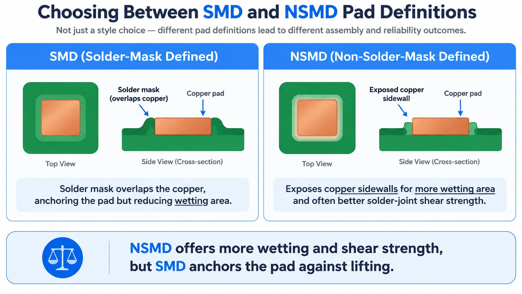
The trade-off is genuine, as the SMD versus NSMD comparison at LTPCBA sets out. NSMD pads expose the copper sidewalls, which increases effective wetting area and often improves solder-joint shear strength and thermal-cycle behavior. SMD pads, where the resist laps the copper edge, mechanically retain the land and reduce pad lifting and cratering under severe mechanical stress and rework.
Read the two wins carefully, because they happen at different depths of the structure. Joint strength is a solder and interface property. Pad retention is a laminate and adhesion property. A pad style that improves the first can degrade the second, which is why calling either one universally superior is a category error.
Product loading decides which side of that trade matters more. The same comparison notes that thicker PCBs improve SAC305 drop-shock reliability by reducing board flexure, and that solder mask can reduce trace-failure risk. Pad geometry alone doesn't determine reliability, and neither does mask style on its own.
<a id="a-per-location-decision-instead-of-a-house-rule"></a>
A Per-Location Decision Instead of a House Rule
- Package size and ball count: a 0.4 mm pitch BGA and an 0805 resistor don't deserve the same definition.
- Board thickness and support: a thin board in a chassis with few standoffs flexes more, and flexure is what lifts pads.
- Drop and vibration exposure: handheld and portable products load the outer rows hardest.
- Rework exposure: a pad that will be reworked twice needs more mechanical retention than one that never sees an iron.
- Copper adhesion: finish, laminate and copper roughness decide how well the land holds before any solder arrives.
Treat corner and outer-row balls separately from inner balls. They carry the highest strain in bend and drop, they're the sites that lift first, and a mixed SMD corner with NSMD interior is defensible when you can say why.
The deliverable that settles this isn't a debate, it's evidence: bend test, drop test, thermal-cycle data, cross-sections and failure analysis for the specific stack. For automotive, industrial, medical and portable products, ask for that package before waiving a review, because a pad that prints beautifully and wets perfectly can still fail beneath the copper-to-laminate interface.
<a id="when-via-in-pad-is-safe-to-use"></a>
When Via-in-Pad Is Safe to Use
"Via-in-pad" is not one construction, and treating it as one is how builds go wrong. A filled and capped microvia under a fine-pitch BGA is a different object from an untreated through-via sitting at the edge of a passive pad, even though both are a hole inside a copper shape, as practical guidance on vias in pads points out.
Two mechanisms matter. Solder paste printed over an open via wicks down the barrel and away from the joint, leaving a starved fillet with a void where metal should be. And on 0402 and 0201 passives, a nearby via can produce unequal wetting forces or thermal asymmetry across the part, which is a tombstone waiting for a profile to trigger it.
| Part and pad | Via construction | Main risk | Decision | |---|---|---|---| | Fine-pitch BGA pad | Filled and capped microvia | Lower wicking risk when filled and planarized | Allowed with plating and planarization spec | | Fine-pitch BGA pad | Open through-via | Solder wicking away from the joint | Avoid and reroute | | 0201 or 0402 passive pad | Open via beneath paste | Solder wicking and tombstoning | Keep the via off the pad | | 0402 passive pad | Filled and capped via | Reduced wicking, but thermal asymmetry remains | Use only after a reflow profile check |
<a id="the-decision-order-for-a-specific-part"></a>
The Decision Order for a Specific Part
- Classify the part first. A passive is not a BGA, and the risk profile differs before you look at any dimension.
- For BGA pads, specify filled and capped construction, with plating quality and planarization in the fabrication notes. Planarization is what lets the paste deposit lie flat over the via.
- Keep passive pads free of open vias. Route the via off the pad, or move it to the far side of the land, before reaching for a fill spec.
- Write the requirement down. Via diameter relative to pad size, fill and cap spec, solder-mask clearance, paste aperture and the inspection method belong in the same fabrication document, in the same units.
- Re-check the profile. If a filled via stays under a 0402 land, confirm thermal symmetry in the reflow profile rather than assuming the fill solved it.
The contrarian point is worth stating plainly: maximum routing density is not automatically the best design objective. A slightly less dense footprint with symmetric paste deposition and thermal geometry often delivers higher first-pass yield and easier rework than a fully packed one that fights the process at every step.
Prototype or production? A filled via under a BGA can carry a prototype build through hand assembly and inspection. Volume production asks a harder question, whether the fill, the planarization and the X-ray recipe hold across thousands of boards on a line you don't run.
The design that suits a one-off prototype is the one you can inspect completely. The design that suits volume is the one whose weak points are documented, specified and covered by a test step.
<a id="confirm-your-pad-design-before-release"></a>
Confirm Your Pad Design Before Release
Turn everything above into a pass-or-fail gate that runs before Gerber output. It takes an hour and it catches the failures that thermal cycling would otherwise find for you in the field.

- Pad type matches the datasheet land pattern, and the library unit is confirmed as mm or mil.
- Padstack, paste aperture and solder-mask rules release together, as one revision rather than three.
- Every via-in-pad carries a fill and cap specification, with plating and planarization stated in the fab notes.
- SMD or NSMD is recorded per package location, with a one-line reason for the choice.
- Thermal pads have a planned via array into the plane they're meant to reach.
- Test pads are unmasked and reachable by the probe fixture being built.
- Hidden-joint parts have an X-ray or cross-section plan agreed before the first article.
- A DFM review has been run and every conflict closed.
If any item fails, hold the release. None of these are documentation preferences; each one maps to a failure mode that surfaces later and costs more.
The review step matters most when the board carries fine-pitch BGA or hidden joints. Send the padstack, stencil and mask files for a fabrication and assembly DFM review before ordering a prototype run, and get the build plan, inspection method and test coverage confirmed in writing. Every board we produce is manufactured to IPC-2 or IPC-3 standards with 100% AOI, flying probe and electrical testing, which is the floor the checklist above is designed to feed, and our engineering team reviews the fabrication data on each order before it reaches the line. Proceed to Gerber release only once the review comes back with no open conflicts, and align the footprint and clearance conventions behind these checks with published PCB design standards so the review starts from a shared baseline.
Lianyuhong Technology Co.,Ltd builds and assembles the boards these pad decisions end up on: full-turnkey SMT, THT and mixed assembly from 01005 parts through fine-pitch BGA and QFN, with AOI, X-ray and functional test covering the hidden joints that pad geometry alone can't protect, plus layout work with SI/PI simulation and a DFM review before release. Send us your padstack, stencil and mask files and we'll return the conflicts in writing before you commit to a prototype run. Visit Lianyuhong Technology Co.,Ltd to start that review.