
You just plugged in the first boards from the prototype run. The firmware boots, the LED blinks, and the sensor answers. Then a pilot lot of fifty comes back, and three of them reset when the enclosure screws go in. A board that powers on at the bench can still fail once the same design hits a real line.
A PCB assembly board is only as trustworthy as the checkpoints behind it. Paste printing, placement, reflow, through-hole soldering, and inspection each catch a different class of defect, and each one also leaves a gap. If you only watch the final power-up, you miss joints that are weak, voided, or one thermal cycle away from cracking.
This walk-through follows the build the way an assembly engineer would explain it on the floor: what each stage protects, where it fails, and which records prove the process will repeat.
Table of Contents
- What a PCB Assembly Board Is and How It Differs From a Bare Board
- How the Build Runs From Files to Shipment
- Surface-Mount Assembly and Reflow Profiles
- Through-Hole and Mixed Assembly Choices
- Quality Checks Before a Board Ships
- Common Defects and How to Fix Them
- Confirm Your Build Package Before Requesting a Quote
<a id="what-a-pcb-assembly-board-is-and-how-it-differs-from-a-bare-board"></a>
What a PCB Assembly Board Is and How It Differs From a Bare Board
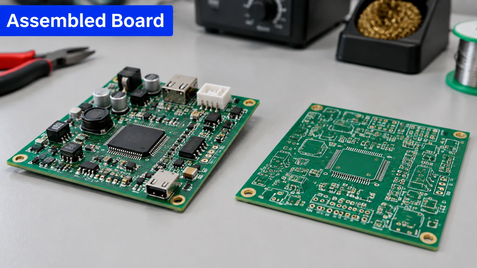
A PCB assembly board is a printed circuit board with its components soldered in place so the circuit can do a job. Think of a bare board as a stage with the wiring already laid out. The assembled board is that same stage with every actor standing on a mark, connected, and ready for the show.
The bare board is only laminate, copper traces, and solder mask. It has pads, holes, and silkscreen, but no resistors, connectors, or chips. It cannot boot, sense, or switch anything until parts are mounted and soldered.
| Attribute | Bare PCB | PCB assembly board | | --- | --- | --- | | Contains | Copper traces, laminate and solder mask only | Traces plus soldered components | | Usually made by | Fabrication house | Assembler, often also sourcing the components | | Main process | Imaging, etching, drilling, plating, solder mask | Solder paste, placement, reflow or wave soldering, inspection | | Tested for | Opens and shorts between nets | Solder joint quality, component placement and working function | | Deliverable | Blank board ready for population | Tested, working board ready for the product |
<a id="two-purchases-one-product"></a>
Two purchases, one product
Those two columns are often two companies. A U.S. Department of Commerce and Bureau of Industry and Security assessment reported that China held a 52.4% share of global PCB manufacturing sales in 2018, about $32.7 billion, and that electronics manufacturing services companies performed 43% of electronic-goods assembly worldwide. Fabrication is concentrated, and a large share of assembly is done by specialists rather than by the shop that etched the copper.
Fabrication builds the substrate and the conductive circuitry. Assembly places and solders the parts, then proves the joints. When you buy a PCB assembly board, you have to specify both halves, including who owns the bare boards, who buys the components, and which tests travel with the shipment.
<a id="how-the-build-runs-from-files-to-shipment"></a>
How the Build Runs From Files to Shipment
Every later checkpoint sits on this sequence. Skip a file or a record, and a later test can only tell you that something failed, not where the process drifted.
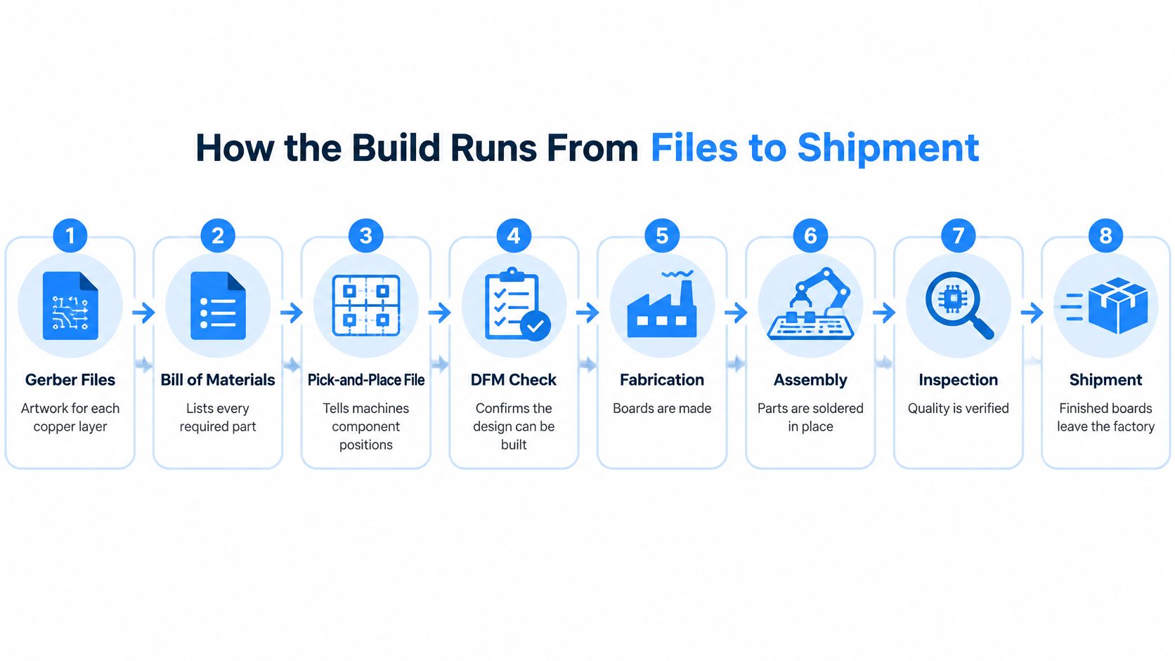
- Files and a design-for-manufacturing check. You send Gerbers, the bill of materials, and the pick-and-place file, and the engineer checks them against the stack-up, footprints, and clearances. A mirrored bottom-side centroid or a footprint that doesn't match the reel part will place every unit wrong.
- Component procurement. Parts are bought and lot status is confirmed before the line starts. An unapproved alternate with a different pad or moisture rating can pass placement and still fail in the field.
- Bare-board fabrication. The fabricator builds the laminate, copper, drills, and mask, or you ship boards in from a partner. A short between nets here looks like a solder bridge later if nobody tests the blank board.
- Solder-paste print and inspection. Paste goes through a laser-cut stencil onto each pad, then solder paste inspection measures volume and position. Paste volume drifts as the stencil wears or as the squeegee pressure creeps.
- Pick-and-place. Machines set chip parts, QFNs, and BGAs onto the wet paste using the centroid file. The usual miss is the wrong reel in a feeder, so a 10 kΩ resistor lands where a 1 kΩ belongs.
- Reflow. The board rides through a nitrogen or air oven on a profile set for that paste and that thickness. A profile copied from a thinner board can leave large thermal pads unmelted.
- Through-hole solder. Connectors and power parts go in after surface-mount, then wave or selective soldering wets the barrels. A missing flux spray or a blocked nozzle leaves pins that look filled from the top and are hollow underneath.
- Inspection and electrical test. AOI and X-ray look at joints, then flying-probe, in-circuit, or functional test checks the circuit. A functional script that only boots the processor will never see an open on an unused pin.
- Clean, pack, and ship. Flux residue comes off when the process requires it, then boards leave with lot numbers and test results. A missing lot record means you can't trace a bad reel after the product is in the enclosure.
A short prototype PCB assembly run uses the same order, just with more hand setup and fewer boards to hide a mistake.
A board passes when every checkpoint is recorded, not when the last test happens to light an LED.
<a id="surface-mount-assembly-and-reflow-profiles"></a>
Surface-Mount Assembly and Reflow Profiles
Surface-mount work is three actions in a row. You print paste, you place parts, and you melt the paste in an oven. Each action protects a different part of the joint, and a defect born at print time is expensive to see after the metal has frozen.
<a id="paste-volume-and-placement"></a>
Paste volume and placement
Stencil printing pushes paste through apertures cut to each pad. Aperture size and stencil thickness set how much solder each joint gets. Too much paste bridges fine-pitch leads. Too little paste starves the joint so it never wets the lead.
Placement has to land small chip parts on both pads, and it has to seat fine-pitch QFN and BGA packages within the pad window. A QFN with a large thermal pad is a useful test of both steps. If you print that pad as one big block of paste, gas gets trapped, the part can float, and the joint voids. Split the thermal pad into several smaller apertures so volatiles can escape and the package stays flat. Stencil aperture rules are covered in more depth in this PCB stencil manufacturer note.
<a id="four-zones-and-the-metal-they-form"></a>
Four zones and the metal they form
The oven is not one temperature. For lead-free SAC305 paste, the board moves through four zones. IPC technical guidance describes soldering as a metallurgical bond formed through intermetallic-compound growth. Too little heat, or poor thermal transfer, stops the solder from wetting. Too much heat, or too long a dwell, grows excessive intermetallic and can damage the component or the laminate. The same IPC test work found that lead-free SMT joints can match tin-lead integrity when paste, laminate, surface finish, and the thermal profile are chosen carefully.
| Zone | Typical range for SAC305 | Purpose | | --- | --- | --- | | Preheat | Ramp of about 1 to 3°C per second toward 150°C | Evaporate solvent and reduce thermal shock | | Soak | About 150 to 200°C for 60 to 120 seconds | Activate flux and even out component temperatures | | Reflow | Peak about 235 to 250°C, with time above the 217°C liquidus | Melt the solder and form the joints | | Cooling | Down below 100°C at 2 to 4°C per second | Solidify joints with a fine grain structure |
Preheat keeps a thick board and a tiny chip from shocking at different rates. Soak lets flux clean the pads and pulls temperatures together so a connector and a 0402 reach liquidus closer together. Reflow is where the alloy melts and wets. Cooling locks the grain. Cool too slowly and the joint coarsens. Cool in a blast and you can crack a ceramic body.
Profile each assembly family on the actual board, with a thermocouple on a large pad and on a small one. Solder paste inspection checks the print that feeds that profile, and X-ray checks the BGA and QFN joints the camera can't see. Those checks belong in the inspection chain, not as a substitute for the profile log.
<a id="through-hole-and-mixed-assembly-choices"></a>
Through-Hole and Mixed Assembly Choices
Through-hole parts put leads through drilled, plated holes. Solder on the opposite side forms a pin-to-barrel bond. That bond is why connectors, power transistors, and heavy electrolytic capacitors still use leads when everything else on the board is a chip.
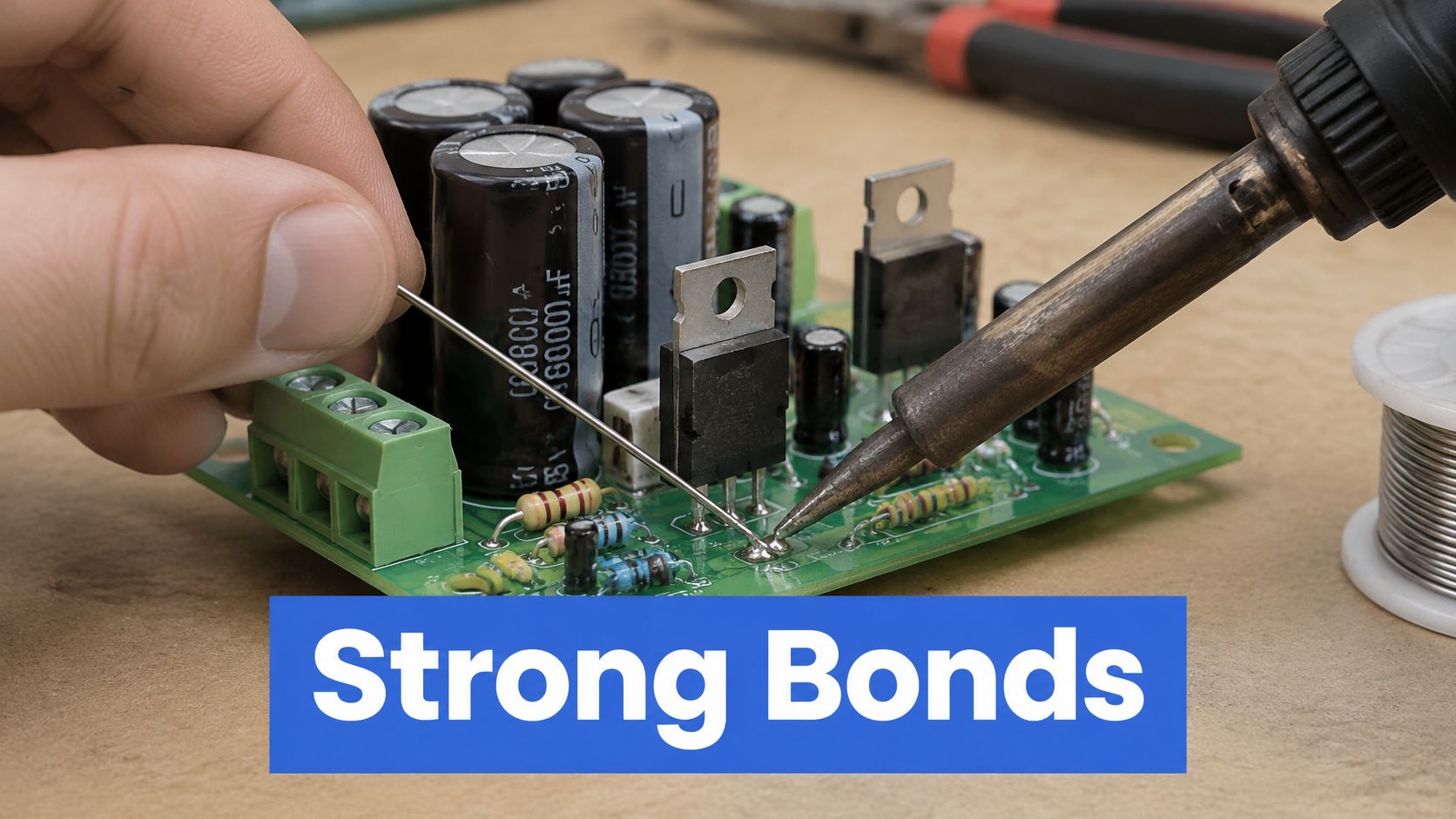
Wave soldering drags the board across a standing wave of molten solder. It suits a side with many pins and few parts that can't take the heat. Flux and preheat come first, or the barrels fill halfway and look acceptable from the top.
Selective soldering uses a small nozzle and a programmed path. You solder the joints you choose and leave heat-sensitive parts alone. It is slower than a wave, and it is the right tool when only a connector and a terminal block need leads.
<a id="most-products-are-mixed"></a>
Most products are mixed
Mixed assembly is the usual case. Surface-mount runs first, often on both sides, with the lighter side reflowed before the heavier one so parts don't fall off on the second pass. Through-hole parts go on after that, by wave or by selective solder. Glue or a fixture holds tall parts if they must survive another heat cycle.
| Criterion | SMT | Through-hole | Mixed assembly | | --- | --- | --- | --- | | Typical components | Chip resistors, QFN, fine-pitch BGA | Connectors, power parts, large electrolytic capacitors | Both types on one board | | Size or pitch | Small chip parts up to fine-pitch BGA | Larger bodies with leads through plated holes | Fine-pitch SMT plus larger through-hole parts | | Mechanical strength | Good for flat parts, weaker under repeated stress | Strong pin-to-barrel bond | Pin strength on connectors, pad strength on chips | | Solder method | Reflow | Wave or selective soldering | Reflow, then wave or selective | | Best for | High-density consumer and IoT boards | Connectors and high-current parts | Most real products |
Use through-hole when the part carries high current or sees repeated mechanical stress. A USB connector that users plug every day is the classic case. Use SMT when you need density and a machine can place thousands of parts an hour.
Through-hole adds a separate solder step, plus fixtures or pallets that keep the wave off the chips. That extra step raises labor and lead time even when the connector itself is cheap. Hand soldering still covers the odd wire or a part that can't go through either machine, and it doesn't scale the way the other two do.
<iframe width="100%" style="aspect-ratio: 16 / 9;" src="https://www.youtube.com/embed/-i2xBAWjUBY" frameborder="0" allow="autoplay; encrypted-media" allowfullscreen></iframe><a id="quality-checks-before-a-board-ships"></a>
Quality Checks Before a Board Ships
No single test covers a PCB assembly board. Each check sits at a point in the line, and each one is blind to something the next check might see. Read the chain in production order, not as a menu you can swap.
Solder paste inspection runs right after print, before any part is placed. AOI runs after placement and again after reflow, comparing the board with a trained image. X-ray looks under packages whose joints face the board. Electrical test comes last, once the metal has frozen and rework is slower.
| Check | Catches | Misses or limits | | --- | --- | --- | | Solder paste inspection (SPI) | Missing, bridged or offset paste before placement | Cannot see the finished solder joint | | Automated optical inspection (AOI) | Missing, misaligned or tombstoned parts, visible bridges | Cannot see joints hidden under BGA or QFN | | X-ray inspection | Voids, opens and bridges under BGA and QFN | Slower and costlier, so often used by sampling | | Flying probe test | Opens, shorts and wrong component values | Needs accessible test points, slower at high volume | | In-circuit test (ICT) | Shorts, opens and component faults using a fixture | Fixture cost, poorly suited to short runs | | Functional test | Whether the board performs its intended job | Does not locate the fault, needs test software |
<a id="a-power-up-is-not-a-process"></a>
A power-up is not a process
A board that boots only proves that the nets in the test script were connected on that unit, on that day. It doesn't prove the paste volume was stable, that the profile reached liquidus on the big pad, or that the next lot of BGAs will wet the same way.
Repeatability lives in the records, not in the green LED.
- First-article inspection compares the first built units with the drawings and the BOM before the lot continues.
- SPI defect distributions show whether paste volume is drifting, not just whether one board failed.
- AOI false-call rates tell you whether the program is finding real defects or training operators to ignore alarms.
- X-ray sampling covers hidden joints you can't afford to image on every board.
- Paste and reflow-profile logs tie each lot to the stencil and the oven recipe.
- Component lot traceability links a reel to the boards that used it.
- Test-fixture coverage lists which nets the fixture touches.
Hand-reworked pads and selectively sourced parts make prototype yield look better than the production process. Those boards no longer match the line you will run at volume, so don't treat their pass rate as a forecast.
A capable PCBA manufacturer should answer three questions before you release the design: which checks run on every board, which checks run by sampling, and where the records are kept.
<a id="common-defects-and-how-to-fix-them"></a>
Common Defects and How to Fix Them
Tombstoning is a defect that is easy to recognize. A small chip stands on one end because one pad wet and pulled harder than the other. Uneven paste, unequal pad size, or a ramp that heats one side first will do it. Balance the pads and slow the ramp so both ends reach liquidus together.
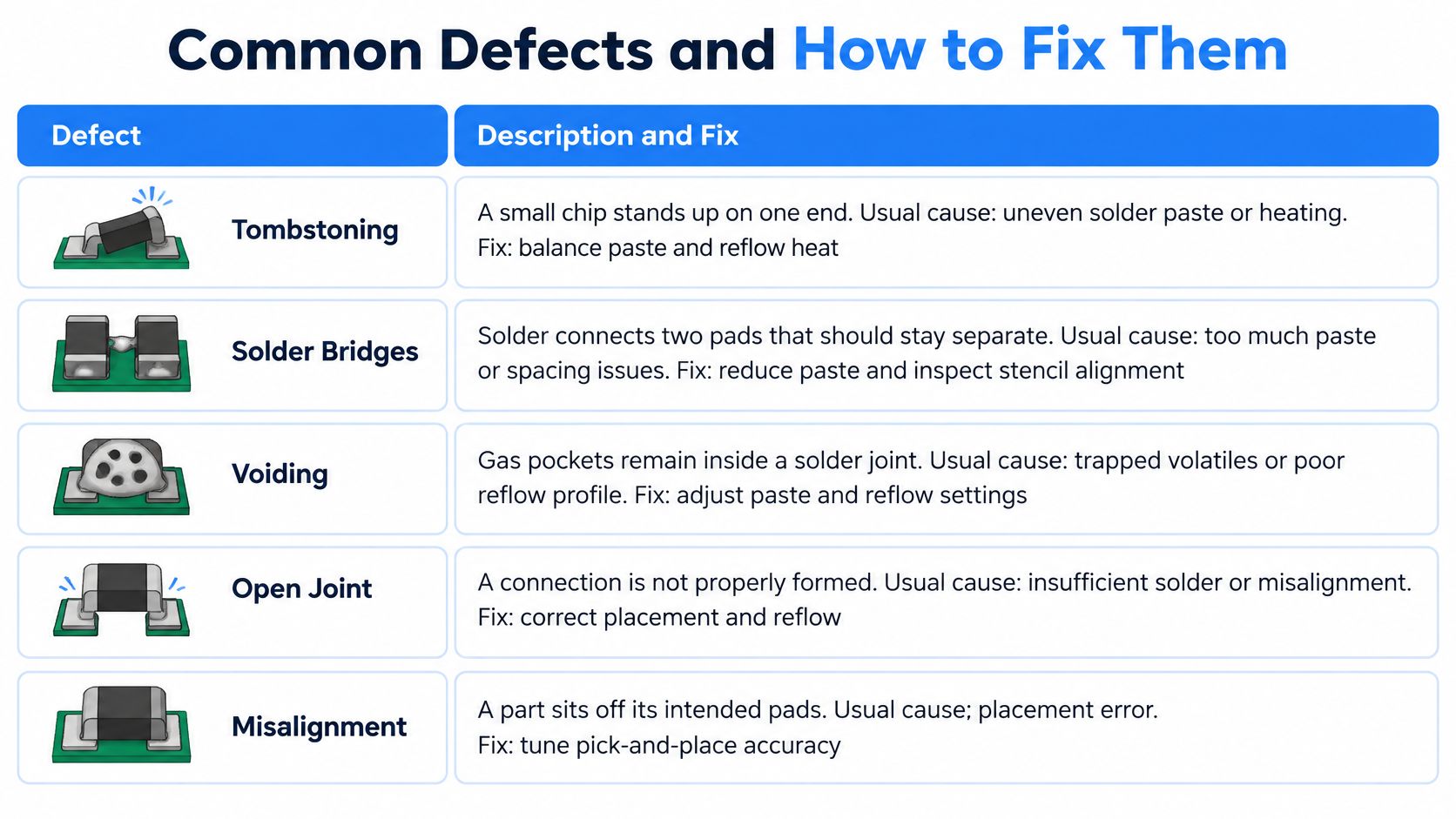
| Defect | Usual cause | Fix | | --- | --- | --- | | Tombstoning | Uneven pad heating or mismatched pad sizes | Balance pad design and tune the reflow ramp | | Solder bridge | Too much paste or oversized stencil apertures | Reduce aperture size and check SPI volume | | Voiding under BGA or QFN | Flux outgassing, cold profile or paste issue | Adjust soak time and review paste and profile | | Cold or dull joint | Insufficient heat or poor wetting | Verify time above liquidus and surface finish | | Lifted pad | Excess heat, repeated rework or weak adhesion | Limit rework dwell time and improve pad design | | Wrong polarity | Placement program or reel error, unclear silkscreen | Check the placement program and polarity marking | | Insufficient fill in through-hole | Too little flux or preheat, poor hole design | Adjust wave or selective soldering parameters |
A bridge is a print problem until proven otherwise. Check SPI volume before you blame the oven. Voids under a BGA usually mean the soak didn't let flux gas out, or the profile never fully melted the center balls. A dull joint needs time above liquidus and a clean finish, not more paste. A lifted pad is often rework heat on a pad that was already thin. Wrong polarity is a data problem: the program, the reel, or a silkscreen dot nobody can see. A through-hole barrel that isn't filled needs flux, preheat, or a hole sized for the lead, not a hotter iron waved over the top.
<a id="the-layout-can-manufacture-the-crack"></a>
The layout can manufacture the crack
Some failures never start at the solder pot. Unsupported leads, a thin annular ring, and copper piled on one side of the board turn vibration and thermal cycling into solder fatigue. NASA workmanship guidance treats IPC-2221 as a common design baseline, with IPC-2222 for rigid organic boards and IPC-2223 for flexible boards. It also says mechanical stress relief should be designed into the joint. Where that relief is missing, a plated-through hole may be mandatory in the constructions those requirements cover.
Before you release fabrication, check component restraint, pad-to-lead geometry, via placement, copper balance, thermal relief, and whether an inspector can see the joint.
Say a sensor board passes every bench test, then drops out after the unit is shaken in its housing. The tall electrolytic has no clamp, and its pads are smaller than the lead needs. Changing the reflow profile won't hold that can down. Add a mechanical restraint and resize the pads, then run the same vibration and the same inspection again.
Change one variable at a time. If you edit the stencil and the profile in the same lot, you won't know which edit fixed the bridge.
<a id="confirm-your-build-package-before-requesting-a-quote"></a>
Confirm Your Build Package Before Requesting a Quote
A quote is only as solid as the package behind it. Pull these six items together before you ask for a price, and you avoid a hold while someone guesses a rotation or a test limit.
- Gerbers, stack-up, and drills. Include copper, mask, paste, silkscreen, outline, and the drill file that matches that revision.
- A complete bill of materials. Manufacturer part numbers, approved alternates, and whether you want reels or cut tape.
- A pick-and-place file. Designators, coordinates, rotation, and side, matched to the same designators as the BOM.
- The assembly type. SMT only, through-hole, or mixed, and which side carries the heavier parts.
- Inspection and test scope. Say whether X-ray covers every BGA and QFN or a sample, and attach the functional procedure.
- A quantity plan. Prototype count, the production quantity, and the lead time you need.
<a id="three-ways-to-split-the-work"></a>
Three ways to split the work
We run three engagement models. Full turnkey means we fabricate the bare boards, source the parts, and assemble them. Consigned full-kit means you supply the boards and the components, and we run SMT and through-hole while keeping the assembly records. Partial turnkey means we fabricate the boards and source the hard-to-find parts, while you supply the rest, with records on everything we buy.
Prototype turnkey assembly can ship in 24 hours when the components are in stock. Standard builds take 2 to 5 business days. Volume production typically takes 7 to 15 business days, depending on component availability and how complex the board is. Confirm how the laminate for your thickness and copper weight is allocated, which substitute materials are already approved, and how a shortage would move both the date and the cost. A stack-up that exists in only one mill can stop an otherwise buildable design.
Lianyuhong offers turnkey PCB assembly, including bare board fabrication, component sourcing, and full assembly under one quality system and one point of accountability.
Send the package for a design-for-manufacturing review and a quote. When the findings come back, check them against the inspection list: every-board checks, sample checks, and where the records will live. That is the difference between a board that powers on once and a PCB assembly board you can build again.
Lianyuhong Technology Co.,Ltd builds and assembles PCB assembly boards from prototype through production, including SMT, through-hole, and mixed technology with paste inspection, AOI, X-ray, and electrical test. If your files, BOM, and test scope are ready, send them for a design-for-manufacturing review and a quoted build. Visit Lianyuhong Technology Co.,Ltd to start that package.