
Your schematic passes ERC, the enclosure is at the printer, and the buyer wants a four-layer board quoted by Friday. You have no EDA license, no budget line for one, and no intention of letting a trial build stamp a watermark on your Gerbers.
That's the moment many start hunting for the best PCB design software free of licensing cost, and the honest answer is that nearly all of it will produce a usable Gerber. The differences show up at the edges. A pin cap that trips halfway through layout. A license clause that bans commercial work. An account requirement that parks a client's design on someone else's server. An export list that stops at Gerber and never writes the NC drill file your fabricator asks for.
This list is sorted by the things that stop a project. License scope first, then the hard caps on layers, pins, accounts and file formats, then the boards each tool realistically finishes. If a tool fails the first two tests, the feature list never gets a vote.
One rule before you install anything. The free tier you pick has to hand your fabricator files they can open without you, in a format they already accept. Everything else is preference.
Table of Contents
- 1. KiCad
- 2. EasyEDA
- 3. DesignSpark PCB Explorer
- 4. LibrePCB
- 5. CircuitMaker
- 6. DipTrace Freeware
- 7. Autodesk Fusion for Personal Use
- 8. Horizon EDA
- 9. gEDA PCB
- 10. Fritzing
- Free PCB design tools compared by platform, limits, commercial use, and best fit
- Matching the Free Tool to Your Next Board
<a id="1-kicad"></a>
1. KiCad
KiCad is the only free suite I'd put in front of a paying client without a hedge. Jean-Pierre Charras released it in 1992 at IUT de Grenoble as a bundle of design programs, and the KiCad project overview now describes a single suite covering schematic capture, PCB layout, Gerber inspection, a calculator and a SPICE simulator, with Gerber and IPC-2581 output on Windows, macOS and Linux, under GNU GPL version 3.
There's no paid tier and no per-seat licensing, which matters more than any feature list. A six-layer board with impedance rules and a documented stack-up doesn't hit a wall at 2 a.m. on a Sunday because someone counted your pads.
<a id="what-the-license-actually-gives-you"></a>
What the license actually gives you
The 9.0.0 release in February 2025 added component classes for applying rules to grouped parts, embedded previously external project assets, and widened pad-stack control across copper layers (KiCad 9.0.0 release notes). For controlled-impedance work that pad-stack and net-class control is where the tool earns its keep, and our walkthrough of impedance control PCB stack-ups shows what a fabricator needs attached to the Gerbers.
The real cost is time and libraries. Reviewers on G2 consistently praise the interactive router and the zero license fee, then flag footprint and library management as the weak point once projects get large.
Skip KiCad if a board has to be routed today by someone who has never opened an EDA tool. Download it at kicad.org.
<a id="2-easyeda"></a>
2. EasyEDA
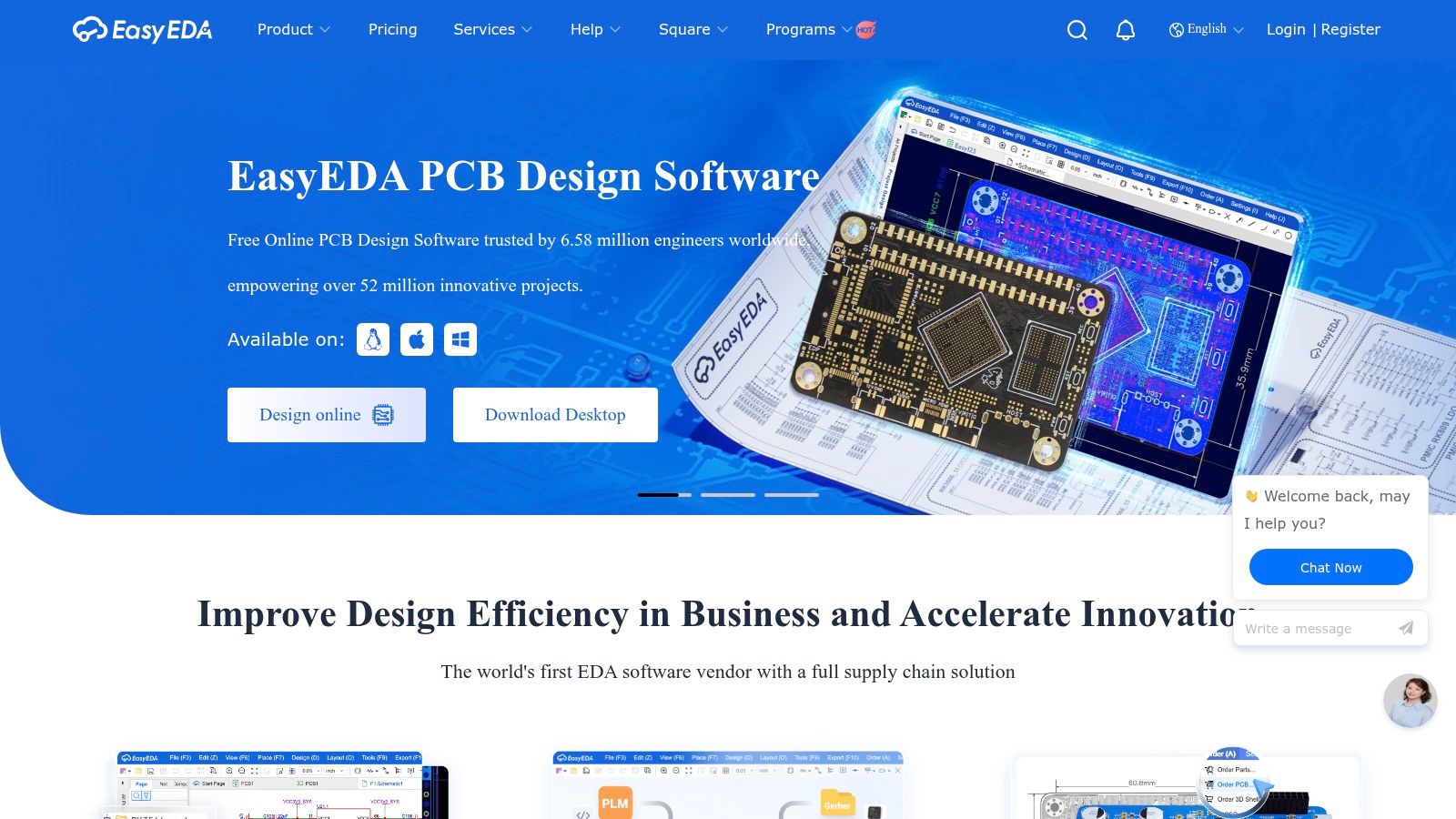
EasyEDA wins on time to first board. Open a browser tab, search a part number, place it, route, export, and the free core never asks for a card. For a two or four-layer prototype that is a fair trade, and the desktop client covers the days when the browser isn't enough.
The editor is a browser tab with a parts search attached, which is why so many first boards start here.
<a id="where-the-free-core-stops"></a>
Where the free core stops
Included: schematic capture linked to layout, a searchable parts library with footprints attached, design-rule checks, Gerber export, and BOM output an assembler can read. Paid: service features around the editor, more storage, and private library control.
The trade is where the design lives and where it leaves. Projects sit in an online workspace and the manufacturing flow nudges you toward one fabrication partner. That's fine for an open dev board. It's a problem when the client's NDA says the files don't leave your machine.
If your data policy forbids cloud storage but your timeline forbids a two-week learning curve, keep EasyEDA for the schematic draft and re-export early. Rebuilding a half-routed board is worse than redrawing a schematic.
Skip it if you work under NDA, in medical or defense programs, or need design files that live only on your own disk. Start at easyeda.com.
<a id="3-designspark-pcb-explorer"></a>
3. DesignSpark PCB Explorer
DesignSpark PCB Explorer is the free tier that reads like a commercial license with the invoice lost in the post. Commercial use is permitted, you keep ownership of your IP, and Explorer produces manufacturing plots and reports instead of stopping at a preview.
Explorer looks like a traditional desktop tool and behaves like one.
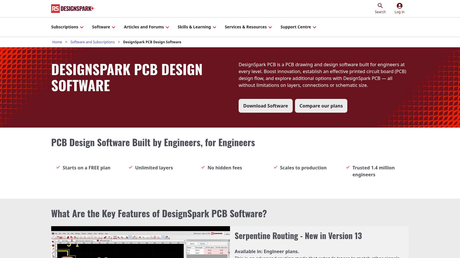
In the box: schematic capture, PCB layout, design-rule checks, 3D viewing, BOM generation and local project files, with no stated layer-count cap on the free plan. That combination is rarer than it should be.
<a id="two-features-that-push-you-to-paid"></a>
Two features that push you to paid
Differential pairs and blind or buried vias sit behind the paid plans. That single line rules out USB, Ethernet, HDMI, most high-speed routing and any stack-up that needs buried layers.
A two-layer LED driver with a handful of analog nets is comfortable here. A four-layer board with a USB-C front end is not, and you'll discover that at the differential-pair step rather than at the download.
The other gate is the account. Explorer needs a verified DesignSpark account tied to RS, so the download isn't anonymous and procurement may ask questions.
Skip it if your board needs controlled-impedance pairs. Register at DesignSpark PCB software.
<a id="4-librepcb"></a>
4. LibrePCB
LibrePCB's selling point isn't the editor. It's the parts library, which forces you to build a symbol, a footprint and a part as separate linked objects before anything can be placed on a schematic.
The library editor is the first thing you meet, and that's deliberate.
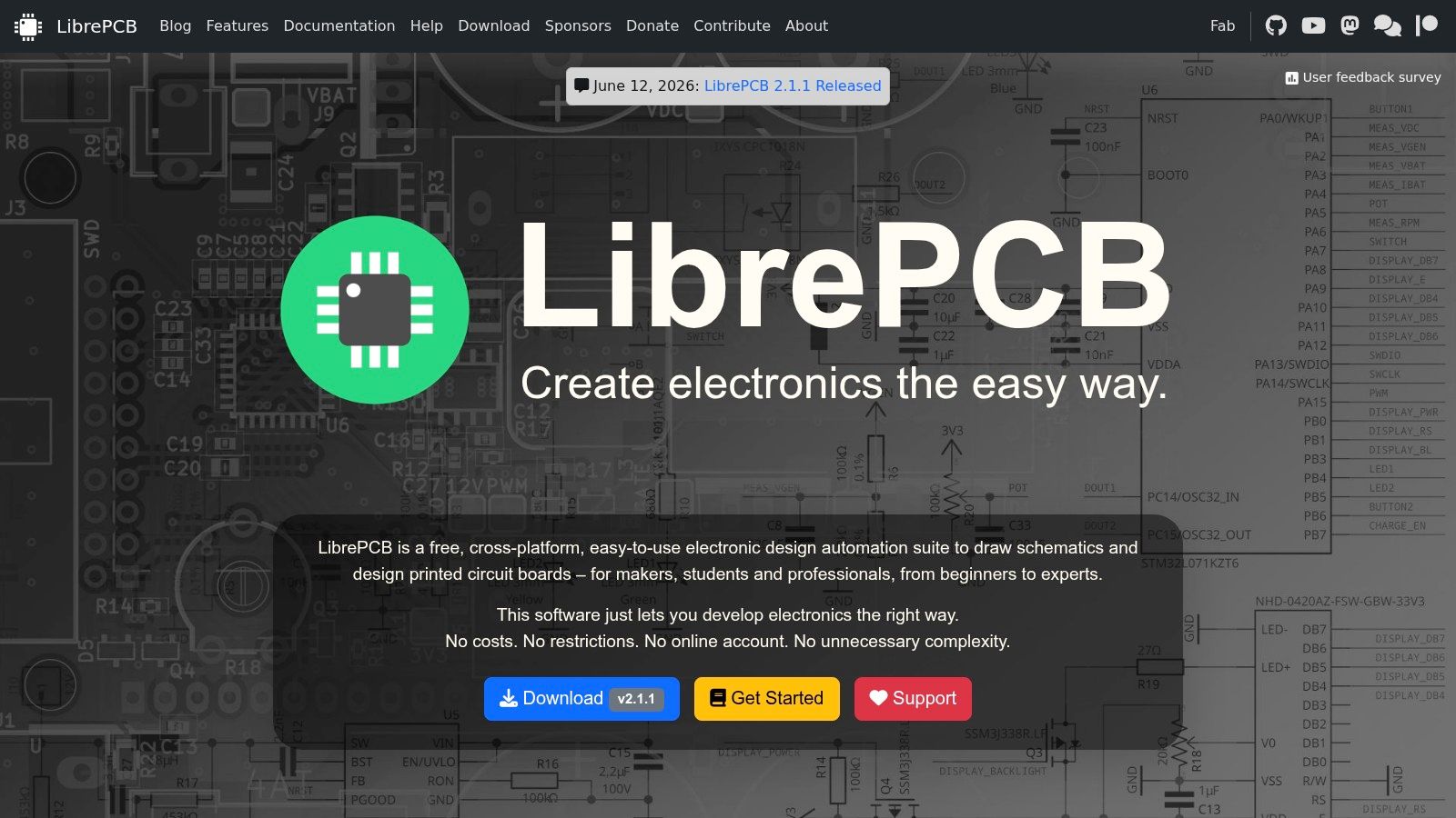
What you get: schematic and PCB editors, cross-platform desktop builds for Windows, macOS and Linux, a structured library format, and no online account at any point. Commercial projects are fine, and the file format is readable enough to keep in version control.
What you don't: the depth of KiCad's ecosystem. Fewer ready-made footprints, fewer tutorials, fewer people who have already hit your bug.
For a first board under a hundred components, the library discipline is a feature. It's the reason a footprint mismatch shows up at review instead of at the assembler.
Free users get the community rather than developer support, so plan accordingly when a release breaks something the week your board is due. Skip LibrePCB if you're designing HDI, RF or anything with tight length matching. Download it at librepcb.org.
<a id="5-circuitmaker"></a>
5. CircuitMaker
CircuitMaker is Altium Designer with the invoice removed, and the routing engine is the reason to look. Push-and-shove routing, differential pairs, multi-sheet schematics and native 3D viewing all come at no cost.
The interface will feel familiar if you've ever opened Altium Designer.
Outputs are production-grade. Gerber, NC Drill and ODB++ all leave the tool, so the format question usually ends here.
<a id="account-workspace-and-who-can-see-your-design"></a>
Account, workspace, and who can see your design
You register, you design inside Altium's online workspace, and your projects live there. Collaboration is the point of that architecture and also the risk. Read the project visibility and community-sharing rules before a customer's board goes anywhere near it.
Check before you load client work. If a project can be made public by default, a confidential design becomes a disclosure problem, not a licensing problem, and disclosure problems are harder to undo.
Skip CircuitMaker if your employer blocks vendor cloud accounts or if the design can't leave a local drive. Register at Altium CircuitMaker.
<a id="6-diptrace-freeware"></a>
6. DipTrace Freeware
DipTrace Freeware is what I'd reach for when a two-layer board is the whole job and I want a desktop program that behaves like a desktop program. The freeware edition doesn't expire, works offline, and the paid upgrades are perpetual licenses rather than subscriptions.
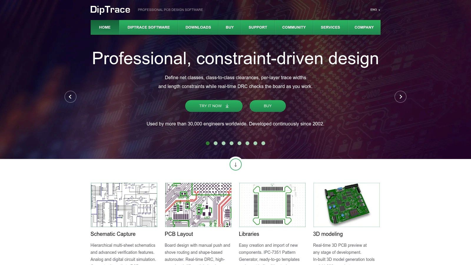
A conventional desktop layout with a parts library down the side.
<a id="the-300-pin-ceiling-in-practice"></a>
The 300-pin ceiling in practice
The cap is 300 pins and two signal layers. That sounds generous until you count a 48-pin microcontroller, a connector, a regulator, a crystal and thirty passives. A sensor node fits. A board with an MCU, USB, an SD card and an LED driver doesn't.
Pins and layers are the two numbers that decide whether PCB design standards can be verified by hand or need tooling, which is why the ceiling matters more than the feature list. The rest of the tool is complete: schematic capture, interactive routing, design-rule checking, component and footprint editors, 3D preview and fabrication outputs.
Two warnings. The freeware terms sit on the non-commercial side, so budget the perpetual license the day the board ships. And Linux use means Wine, not a native build.
Skip DipTrace if the design will grow past two layers in the next year. Download it at diptrace.com.
<a id="7-autodesk-fusion-for-personal-use"></a>
7. Autodesk Fusion for Personal Use
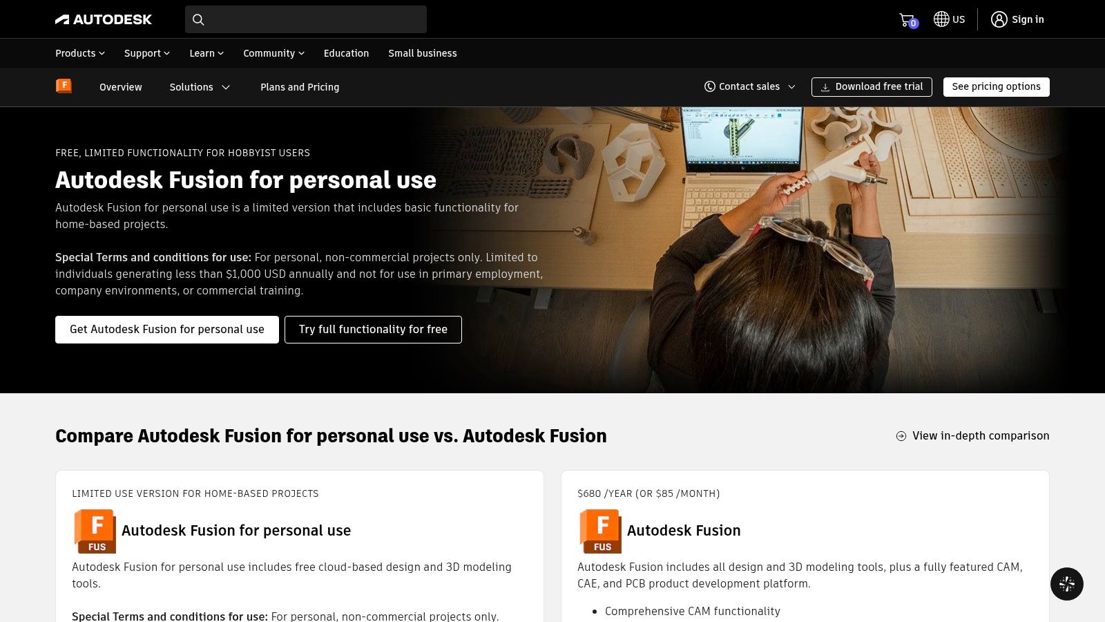
Fusion for Personal Use is what you reach for when the problem is fit rather than routing. The electronics workspace sits in the same file tree as the mechanical model, so a connector that clashes with a case rib shows up before you pay for tooling.
The electronics workspace sits beside your mechanical model in the same project tree.
<a id="where-the-personal-license-ends"></a>
Where the personal license ends
Autodesk's personal-use terms cover home-based, non-commercial projects and exclude company work. The electronics side also caps schematic sheets, signal layers and total board area compared with paid Fusion, and document limits apply to how many files stay active and editable in the cloud.
That combination is fine for a one-off enclosure fit check. It's not a route to a product. If a startup designs inside Fusion Personal and then tries to ship, the license is the problem before the layer count is.
Skip it if the board belongs to a company, a client or a revenue plan. Check the terms at Fusion 360 for personal use.
<a id="8-horizon-eda"></a>
8. Horizon EDA
Horizon EDA is built around one idea. A shared pool of parts that every project draws from, so a part approved once is approved everywhere, with schematic, layout, 3D preview and fabrication export working from the same data.
The part pool is visible from every editor, which is the whole architecture in one screen.
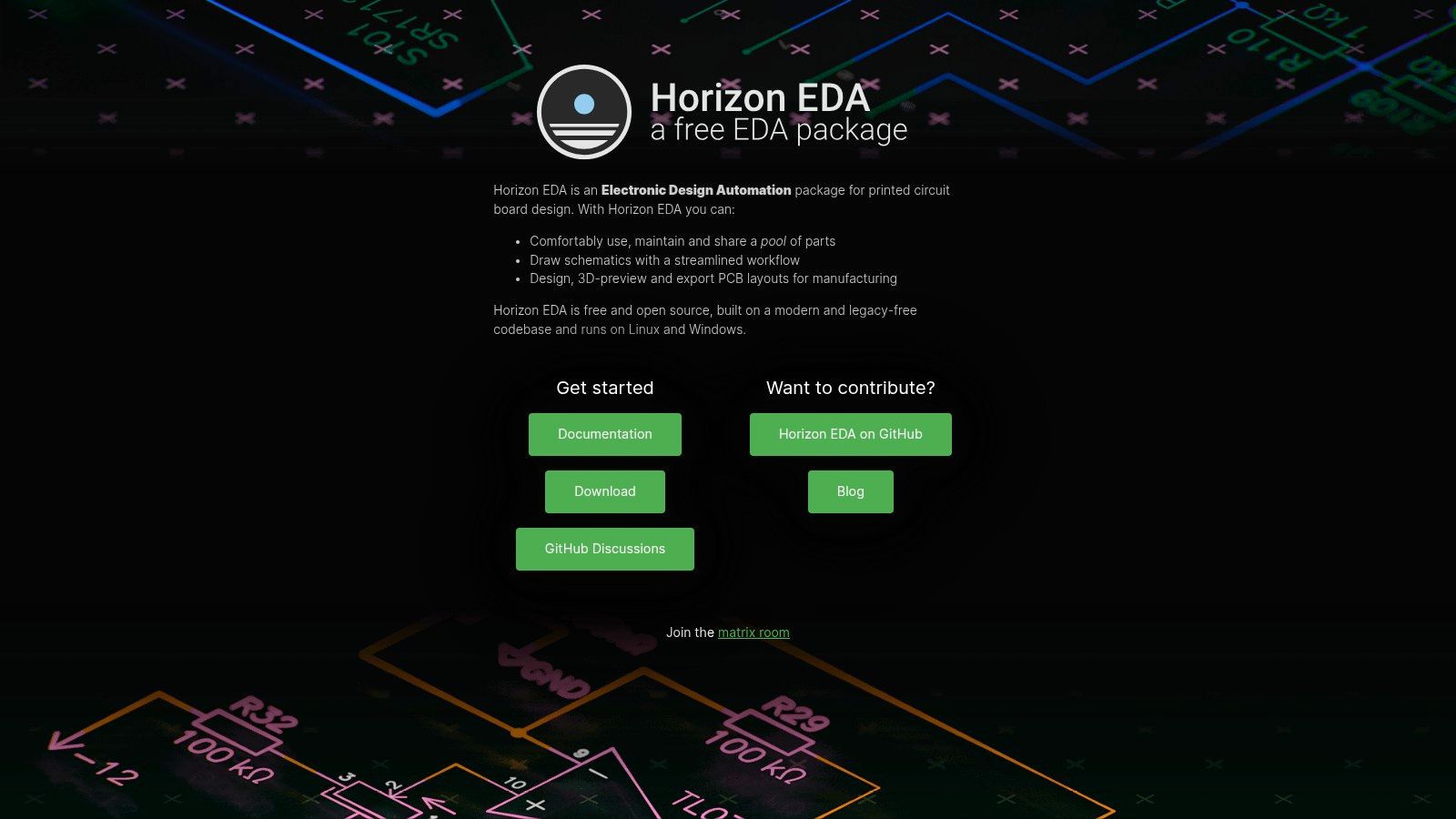
Strengths: free and open source, integrated schematic, parts and layout, 3D preview, and manufacturing export without a paid tier. The gap: a smaller community and thinner learning material than KiCad, and macOS isn't listed among supported platforms.
That last point ends the conversation for a lot of Mac-based teams. For a Linux engineering group that wants strict part control across several designers, it's a genuine alternative to fighting KiCad's library habits.
Skip Horizon EDA on macOS, or if you'll need a forum answer within the hour. Start at horizon-eda.org.
<a id="9-geda-pcb"></a>
9. gEDA PCB
gEDA PCB is the layout half of a modular toolchain. A schematic front end writes a netlist, PCB reads it, and you route from there, with ratsnest support and design-rule checking along the way.
<a id="what-a-modular-toolchain-costs-you"></a>
What a modular toolchain costs you
What it does well: Gerber and NC drill output, established file formats, lightweight operation on old hardware, and layout that can be scripted because each stage is a separate program with a text interface.
What it costs: the interface is older than most of the people using it, documentation is scattered across tools, and setup assumes you're comfortable with a Unix workflow. Newcomers burn a weekend before the first board exists.
A modular toolchain isn't a flaw. It's a workflow choice that rewards engineers who automate, and punishes anyone who expects one installer and one window.
Skip gEDA PCB if you want an integrated environment where the schematic and the board stay in sync automatically. It's for people who already live in this ecosystem or need the scriptability. Start at geda-project.org.
<a id="10-fritzing"></a>
10. Fritzing
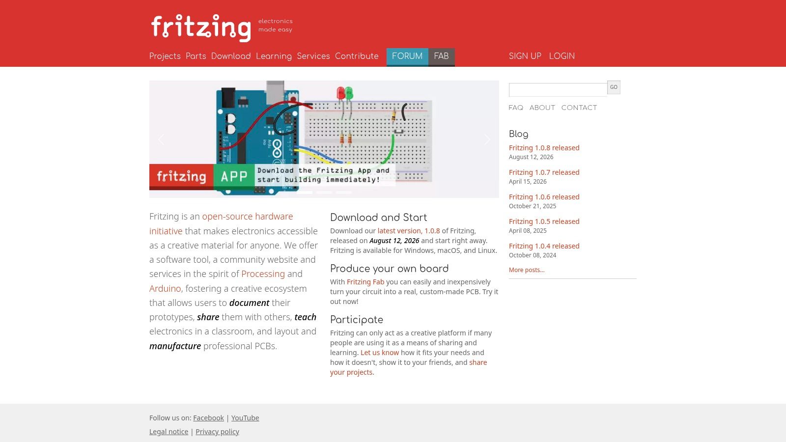
Fritzing's breadboard view is the best teaching device in this list. It's also the strangest license structure, because the compiled installers require a purchase or contribution while the source code stays available for anyone willing to build it.
The three views below are the reason it survives in classrooms.
<a id="paid-installers-and-free-source"></a>
Paid installers and free source
What it gives you: breadboard, schematic and PCB views of the same circuit, project documentation and sharing, Windows, macOS and Linux builds, and a fabrication workflow for simple boards.
What it won't do: tight, dense or high-frequency layouts. The physical-looking breadboard view is a documentation tool, not a constraint engine, and there's a reason production boards don't come out of it.
For teaching and for documenting a build, the visual approach earns its place in PCB design projects where the circuit has to be explained to someone who doesn't read schematics.
Skip Fritzing for anything going into a product enclosure, and don't expect a free download link on the site. Check the current release terms at fritzing.org.
<a id="free-pcb-design-tools-compared-by-platform-limits-commercial-use-and-best-fit"></a>
Free PCB design tools compared by platform, limits, commercial use, and best fit
Free means something different in every row below. Two columns decide most eliminations before a schematic is even drawn: the cap on pins, layers or documents, and whether the license lets you ship paid work.
| Item | Platforms | Free Limits | Commercial Use | Best For | |---|---|---|---|---| | KiCad | Windows, macOS, Linux | No caps; the full toolset is free | Suitable for commercial and production designs | Full-featured, fabrication-ready PCB design | | EasyEDA | Browser and desktop | Free core features; optional paid plans | Core features support commercial designs | Quick browser-based schematic-to-PCB workflows | | DesignSpark PCB Explorer | Windows desktop | Free plan; some advanced features require paid plans | Permitted for commercial use | Free design with manufacturing outputs | | LibrePCB | Cross-platform desktop | No caps; entirely free | Free for commercial projects | Open-source design with an approachable workflow | | CircuitMaker | Windows desktop with a cloud workspace | Free tool; registration and online workspace required | Review project-sharing rules for confidential work | Advanced routing and collaborative PCB design | | DipTrace Freeware | Desktop; Linux via Wine | 300 pins and two signal layers | Freeware is non-commercial; a shipped board needs a perpetual paid license | Modest boards and offline design | | Autodesk Fusion for Personal Use | Windows and macOS desktop; cloud storage | Limited personal-use features and active/editable documents | Noncommercial use only; excludes company work | Hobby projects needing PCB and 3D CAD coordination | | Horizon EDA | Windows, Linux | No caps; entirely free | Open-source license; commercial work allowed | Integrated schematic, parts, and PCB workflow | | gEDA PCB | Linux and Unix-like desktops | No caps; entirely free | GPL license; commercial use permitted | Lightweight, modular PCB layout and manufacturing output | | Fritzing | Windows, macOS, Linux | Official compiled installers require purchase or contribution; source can be compiled | Open-source license permits commercial use; only the prebuilt installer is paid | Education, breadboard documentation, and simple prototypes |
Read the limits column as a ceiling, not a starting point. KiCad, LibrePCB, Horizon EDA and gEDA carry no ceiling at all. DipTrace's 300-pin, two-layer cap sizes the largest board it can finish, and its license turns into a purchase the moment a board ships commercially. Fritzing sits at the other end of the scale: the license is free, the download is not, and the tool is built for documentation rather than dense layouts.
<a id="matching-the-free-tool-to-your-next-board"></a>
Matching the Free Tool to Your Next Board
Four checks, in this order, and you'll have your answer before lunch.
License scope first. Search the EULA for the word commercial. KiCad's GPL v3 allows paid work, as do LibrePCB and Horizon EDA. Fusion Personal and DipTrace's freeware edition don't. Everything else needs reading rather than assuming, and the reading takes ten minutes against the cost of a redesign.
Then the hard caps. Match the layer and pin ceiling to the board you're planning in twelve months, not the one on your desk. A 300-pin cap or a paid differential-pair feature feels theoretical until a USB port appears on the schematic.
Then the outputs. Confirm the tool writes the formats your fabricator and assembler accept. Gerber alone isn't a handoff. You want NC drill, a BOM, pick-and-place data, and the stack-up and impedance notes that tell the fab what to build. Maintenance belongs in this check too: KiCad 6.0.2 shipped in February 2022 specifically to correct reported vulnerabilities (KiCad 6.0.2 release notes), which is what a project with a security process looks like.
Then the account. Offline continuity and file portability decide what happens when a team changes or a free tier changes. The argument in Rankite's comparison of circuit design software is that tools should be scored on open-file portability, local operation, export completeness and library provenance rather than monthly cost, and that's the right scorecard for anyone who has watched a vendor retire a tier.
The money in this category keeps growing. The Business Research Company, via GII Research, projects the PCB design software market rising from USD 3.49 billion in 2025 to USD 3.93 billion in 2026, a 12.6% compound annual growth rate, and the free tier is still where most first boards get made.
When layout time or fabrication readiness becomes the bottleneck rather than license cost, that handoff is a normal next step. Lianyuhong Technology Co.,Ltd handles PCB layout from $100 per project and accepts native KiCad, Altium, Eagle and PADS files for DFM review, with documented stack-ups and impedance held to ±8 percent, which is usually the number that decides whether a four-layer quote comes back clean.
A free tool gets your schematic into a Gerber. Lianyuhong Technology Co.,Ltd takes it the rest of the way, with rigid, HDI, flex, metal-core, high-frequency and ceramic fabrication in-house plus turnkey SMT and THT assembly that starts at a single prototype board with no minimum order. Upload your Gerber, BOM and pick-and-place files and our engineers return DFM feedback before you commit to a production run. Visit Lianyuhong Technology Co.,Ltd to start a quote.