
A schematic can simulate cleanly and still produce a first prototype that overheats, picks up noise, or won't fit inside its enclosure. The layout decisions that cause those problems are often hard to spot until the board meets real components, cables, power loads, and mechanical constraints. That's why studying completed PCB design projects is useful: each one shows how a specific choice shaped the result, and what you can apply to your own design.
The examples below span beginner, IoT, consumer, and industrial work, from a straightforward microcontroller board to RF, rigid-flex, and ceramic power designs. The boards differ, but the engineering questions repeat: where will current flow, how will heat escape, what needs controlled impedance, and can a fabricator build and inspect the design as released?
Each project focuses on one decision with an outsized effect, followed by a tactic you can adapt. Use the examples as starting points, not templates to copy blindly. Board dimensions, component choices, enclosure, and operating conditions all affect the right design.
Table of Contents
- 1. Raspberry Pi Single-Board Computer Reference Design
- 2. Arduino Uno Open-Hardware Board
- 3. ESP32 Development Board for IoT Products
- 4. Metal-Core PCB for LED Lighting Modules
- 5. High-Frequency RF Power Amplifier Board on Rogers Laminate
- 6. HDI Smartphone Mainboard with Any-Layer Microvias
- 7. Rigid-Flex Wearable Health Monitor
- 8. Ceramic DBC Substrate for Power Electronics Modules
- How the eight PCB design projects compare
- Turn These PCB Design Projects Into Your Next Board
<a id="1-raspberry-pi-single-board-computer-reference-design"></a>
1. Raspberry Pi Single-Board Computer Reference Design
A Raspberry Pi-style single-board computer packs a processor, memory, power circuitry, and multiple interfaces into a compact consumer product. Its central design challenge is making dense, high-speed circuitry work within a low-cost, manufacturable board. A four-layer FR-4 design can support the processor and interfaces while providing reference planes for controlled-impedance routing.
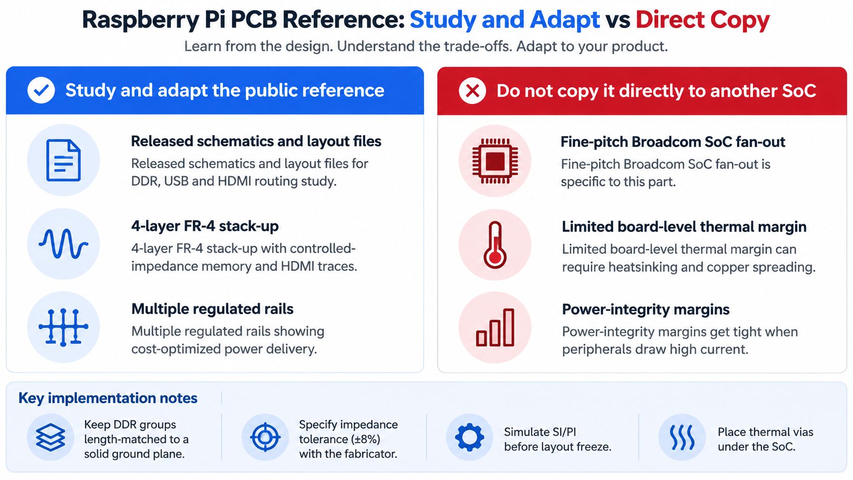
The key decision is the stack-up. DDR memory routing, power delivery, and USB, HDMI, and camera or display interfaces don't all have the same layout needs. A solid ground reference helps keep return currents close to their signal paths, while a deliberate layer assignment makes it easier to route the memory bus without cutting up the plane. Publicly documented schematics and layouts make this kind of board a useful reference, but copying its dimensions or routing without matching its components and fabrication process can create new problems.
<a id="adapt-the-layout-not-just-the-shape"></a>
Adapt the layout, not just the shape
For an industrial IoT gateway built on a similar architecture, start by documenting the stack-up and interface requirements. Keep DDR address and data groups length-matched, reference them to a continuous ground plane, and have the fabricator confirm the specified impedance tolerance. Run signal- and power-integrity checks before the layout is frozen, then plan copper spreading and thermal vias under the processor.
The effort needed to lay out a PCB depends on more than its area. A University of California, Santa Cruz study of PCB layout-time estimation found meaningful correlations between layout effort, board area, and component count, and proposed a broader complexity estimate using variables such as pin count, device types, sizes, and layer count. For a reference design, that's a reminder to inspect the engineering constraints, not just how compact the finished board looks.
<a id="2-arduino-uno-open-hardware-board"></a>
2. Arduino Uno Open-Hardware Board
The Arduino Uno's most instructive decision is its standardized header layout. The board's 8-bit AVR microcontroller and USB-to-serial interface matter, but the header positions are what let users connect a wide variety of shields without redesigning the base board. That predictable electrical and mechanical interface made the Uno useful in classrooms, maker projects, and early product prototypes.
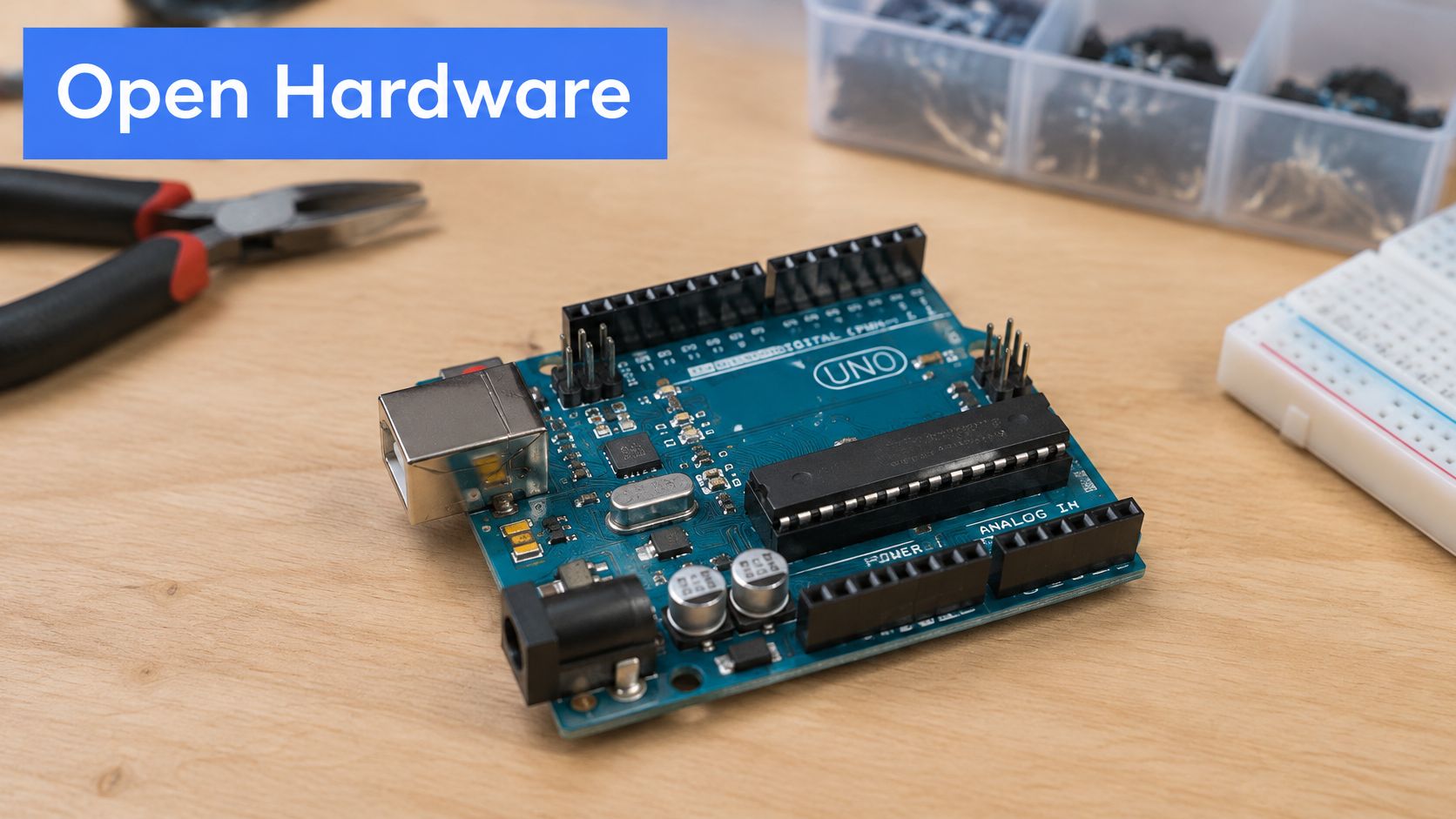
For a custom sensor board, the Uno's header pattern can save time if you need compatibility with existing shields. But using the footprint is only the start. Check what each pin does, how much current your add-on draws, and whether the combined stack of boards will fit inside the enclosure. A connector standard can simplify integration, but it can't fix an unsuitable pin assignment or a power supply that sags under load.
<a id="build-the-electrical-details-in-early"></a>
Build the electrical details in early
Mixed-signal add-ons need thoughtful return paths. Place analog circuitry so its sensitive signals don't share a noisy return path with fast digital edges or switching loads. Make the reset and bootloader path part of the schematic from the beginning, so firmware updates don't depend on improvised wiring after the board arrives.
This design suits a classroom controller, a low-cost industrial control prototype, or a custom sensor board that needs to reuse common modules. Before release, check the two-layer layout against the fabricator's preferred trace widths, clearances, and drill sizes. Keeping the board simple is useful only if it's also easy to build and assemble. A design-rule check and a manufacturing review catch different problems, so do both before ordering.
<a id="3-esp32-development-board-for-iot-products"></a>
3. ESP32 Development Board for IoT Products
An ESP32 development board makes wireless prototypes accessible, but the antenna area is not ordinary board space. A designer who routes copper or places a metal enclosure too close to the antenna can compromise the radio link even when the firmware and schematic are correct. A pre-certified module can reduce some RF design risk, but it doesn't make the antenna placement and surrounding geometry irrelevant.
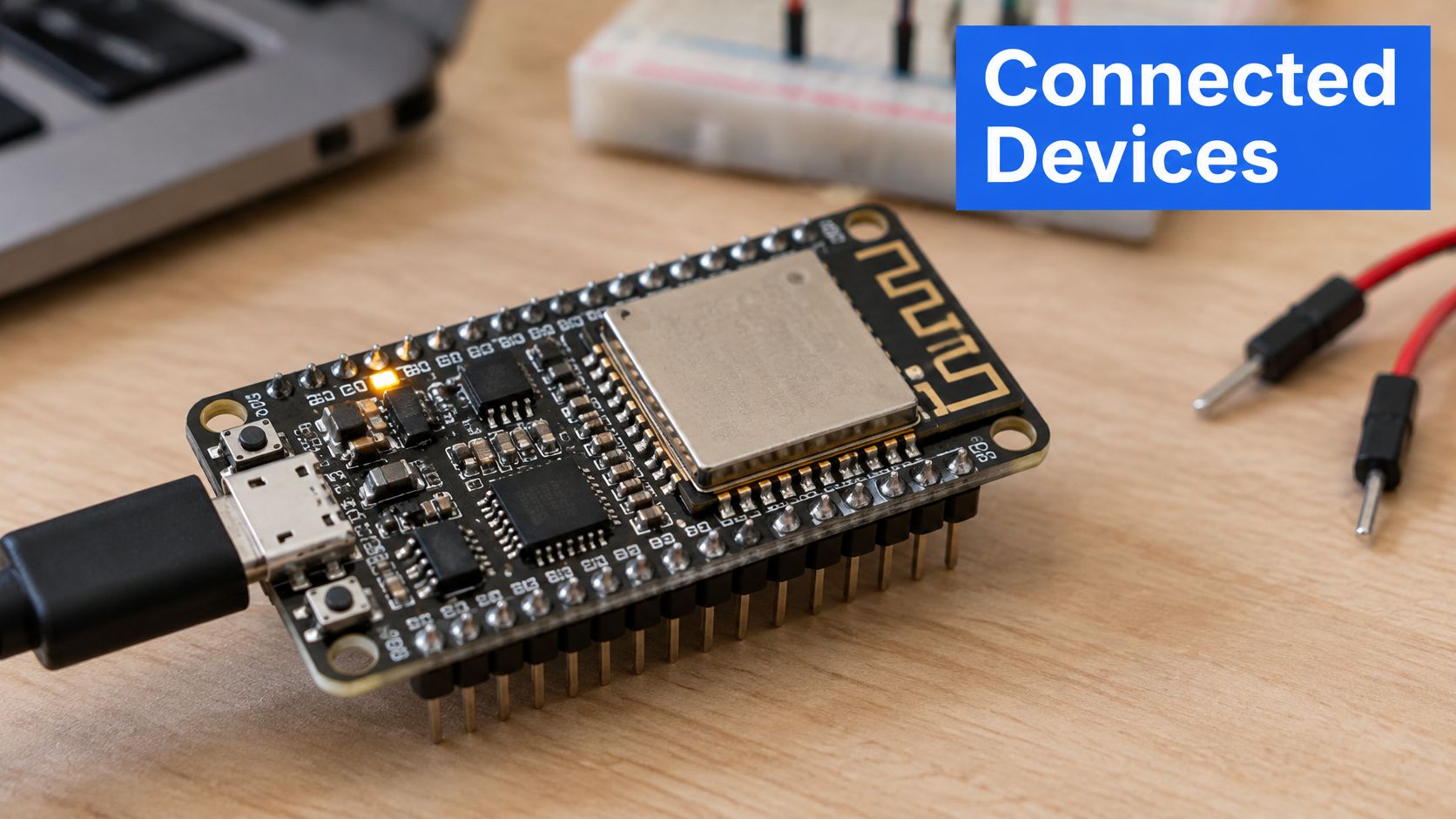
Keep the module vendor's antenna keep-out and ground guidance intact. Place the antenna at a board edge where its radiating area isn't boxed in by copper, batteries, or nearby metalwork. During bring-up, measure the antenna with a VNA or antenna analyzer rather than assuming a successful Wi-Fi connection in one room proves the RF layout is sound.
<a id="design-around-radio-current-bursts"></a>
Design around radio current bursts
A connected environmental monitor or smart-home sensor may appear to be a light-load circuit until the radio transmits. Plan the supply for those bursts, place decoupling close to the module's power pins, and provide enough bulk capacitance to limit voltage droop. A weak power path can cause resets that look like a software fault.
A four-layer stack-up can help organize the power and ground returns while keeping the RF section manageable. Still, no stack-up can compensate for ignoring the antenna's keep-out. If the product uses a plastic enclosure, test the assembled device in that enclosure, because the final geometry affects the radio environment. The practical tactic is simple: preserve the antenna area, then validate the complete assembly rather than judging RF performance from the bare board alone.
<a id="4-metal-core-pcb-for-led-lighting-modules"></a>
4. Metal-Core PCB for LED Lighting Modules
For a high-brightness LED board, the most consequential choice is often how heat moves through the substrate. A metal-core PCB gives heat a path from the LED packages through a dielectric layer to a metal base and, in turn, the fixture or heatsink. That can address a hotspot at the board level instead of relying entirely on external cooling.
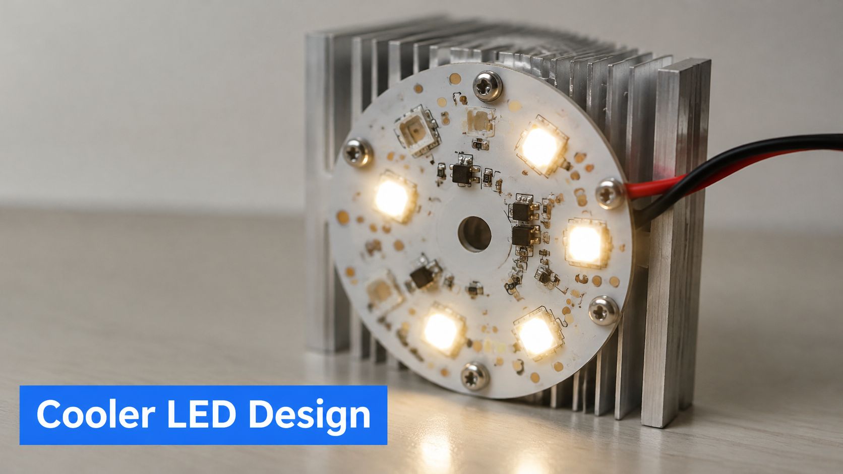
The dielectric's thermal conductivity and thickness affect the thermal path, so choose them with the LED power density and target junction temperature in mind. Copper thickness also matters for current handling, especially on high-current LED strings. If the design combines a thermal substrate with multilayer driver circuitry, thermal vias can help connect the relevant copper regions, but they don't remove the need to consider the whole heat path.
<a id="test-the-assembled-thermal-path"></a>
Test the assembled thermal path
A thermal study comparing equivalent multilayer boards measured a maximum component temperature of about 144°C on standard FR-4 and 118°C on a higher-thermal-conductivity dielectric under the same operating conditions, a 26°C difference. The PCEA thermal PCB design study also found that surface-mount thermal bridges reduced peak temperature on both boards, but offered less relative benefit on the higher-performance dielectric, where heat spread through the board became the dominant path.
For a street-lighting module, test the LED board with its actual thermal interface material, mounting pressure, and enclosure. A good board material can't compensate for poor contact with the heatsink. Use the same load and measurement method when comparing substrate options, copper spreading, thermal vias, and enclosure paths. That gives the team a practical basis for choosing the stack-up, rather than treating a material's datasheet value as the final system result.
<a id="5-high-frequency-rf-power-amplifier-board-on-rogers-laminate"></a>
5. High-Frequency RF Power Amplifier Board on Rogers Laminate
In an RF power amplifier, the material decision shapes what happens to the signal before the amplifier can deliver it to the antenna. Low-loss laminates such as Rogers RO4350B or PTFE-based materials can be appropriate for telecom, radar, and microwave circuits where dielectric loss and impedance control matter. But using a premium laminate alone won't guarantee the expected result. The layout and the actual manufactured stack-up need to match the electrical model.
The replicable tactic is to base simulations on measured or confirmed material properties, not just nominal values. Use SET2DIL or Delta-L methods to characterize dielectric properties when the design demands that level of control, then model transmission lines against the fabricator's documented stack-up. For a hybrid FR-4 and RF-laminate build, confirm bonding and coefficient-of-thermal-expansion compatibility before committing to the stack.
<a id="measure-the-fabricated-board"></a>
Measure the fabricated board
A cellular base-station amplifier is a useful example of why layout and measurement must stay connected. Validate the board on a VNA across the intended operating conditions, and check performance at relevant temperatures and power levels. If measured behavior differs from simulation, review the as-built geometry and material assumptions before making a blind layout adjustment.
For additional manufacturing context, see this guide to Rogers PCB manufacturing. The core lesson is that controlled impedance isn't just a number in a drawing. It depends on geometry, dielectric properties, copper, and the fabrication stack-up working together. Confirm those inputs early, then use measurement to verify the finished board.
<a id="6-hdi-smartphone-mainboard-with-any-layer-microvias"></a>
6. HDI Smartphone Mainboard with Any-Layer Microvias
A smartphone mainboard shows what HDI can achieve when conventional through-hole routing can't fit between fine-pitch packages. Laser-drilled microvias and sequential lamination give designers more options for escaping dense BGAs and routing connections through a thin board. The decisive choice isn't to use microvias. It's to define a stack-up the fabricator can build reliably before the layout depends on it.
For a compact camera or wearable module, decide early where microvias are needed and how they connect across layers. Confirm the allowable aspect ratios and the fabricator's process for stacked or staggered structures. Via-in-pad can help with escape routing, but only when the via can be filled and capped to support component assembly. Otherwise, the pad may not behave as the footprint requires.
<a id="review-escape-routing-before-release"></a>
Review escape routing before release
A practical release review should examine pad sizes, escape routes, microvia placement, and the transitions between layers. For a fine-pitch BGA, don't assume that a clean view of the top layer means the hidden routing is manufacturable. The HDI PCB manufacturing guide provides context on the fabrication side of these structures.
Build inspection into the plan. X-ray can reveal hidden joints and structures that visual inspection can't reach, while electrical testing helps catch opens and shorts. For a smartphone-style board, the tactic is to coordinate stack-up, escape routing, assembly, and inspection before the design is frozen. HDI earns its value when the density solves a real size constraint and the whole production path supports the design.
<a id="7-rigid-flex-wearable-health-monitor"></a>
7. Rigid-Flex Wearable Health Monitor
In a wearable, removing connectors and cables can matter as much as reducing the board outline. A rigid-flex circuit combines rigid islands for components with flexible sections that bend around the body or fit a curved housing. That can simplify assembly and eliminate interconnects that would otherwise need space and mechanical support.
For a health-monitor wristband, place processors, sensors, and connectors on rigid sections, then keep flex regions clear of components and vias. Route traces perpendicular to the bend line where practical, and define the bend radius and expected flexing in the mechanical requirements. Stiffeners can support connector and component areas, but extending a stiffener into a bend region can shift stress to the edge of the supported area.
<a id="treat-the-flex-as-a-mechanical-part"></a>
Treat the flex as a mechanical part
The layer count, coverlay, copper construction, and bend geometry need to be agreed with the fabricator before routing is complete. A design that looks compact in a 2D layout can fail to assemble or flex as intended when the actual enclosure and forming process are considered. For implementation details, use these rigid-flex PCB design guidelines.
Reliability testing should match the product's mission profile, not just confirm that the prototype powers on. A 2025 study modeled PCB assemblies under temperature cycling and random vibration, validated predicted failure locations experimentally, and reported 88.89% failure-prediction accuracy. Its study of PCB assembly reliability under combined stresses also found that a change beneficial under one stress mode could reduce life under another. For a wearable, test the assembled product under the relevant movement and environmental conditions instead of assuming that a mechanically tidy layout guarantees long-term durability.
<a id="8-ceramic-dbc-substrate-for-power-electronics-modules"></a>
8. Ceramic DBC Substrate for Power Electronics Modules
For a power module, the defining decision is whether the substrate can manage heat while electrically isolating the power devices. A direct bonded copper ceramic substrate combines a ceramic base with bonded copper, making it useful in motor drives, inverters, and industrial converters. Aluminum nitride (AlN) suits designs that need higher thermal conductivity, while alumina (Al₂O₃) can be a lower-cost choice when the thermal load allows it.
Copper thickness should match the current requirement, but current capacity is only part of the design. Thermal simulation helps identify hotspots, and the module's soldered or sintered joints must tolerate the mismatch in thermal expansion between materials as temperature changes. A design that optimizes only the ceramic's thermal property can still create reliability risks at interfaces and joints.
<a id="validate-the-module-as-an-assembly"></a>
Validate the module as an assembly
For an electric-vehicle inverter or renewable-energy converter, plan inspection around the hidden interfaces. X-ray can help assess internal joints, while thermal imaging under load can reveal uneven heat distribution. Define those checks during design review, not after the first assembled module.
The useful tactic is to compare substrate options under the same electrical and thermal conditions, then include the interconnects and cooling arrangement in the analysis. Ceramic DBC is not a universal upgrade over FR-4 or metal-core boards. It's a targeted solution for power density, electrical isolation, and heat transfer requirements that the simpler substrate options can't meet. Choose it when the system needs those properties, and validate the finished assembly rather than relying on material selection alone.
<a id="how-the-eight-pcb-design-projects-compare"></a>
How the eight PCB design projects compare
| Project | Board Construction | Primary Application | Main Design Constraint | |---|---|---|---| | Raspberry Pi Single-Board Computer Reference Design | 4-layer FR-4 rigid PCB with controlled-impedance routing and BGA SoC | Educational computing, robotics, and embedded gateways | Signal integrity and power delivery within a low-cost design | | Arduino Uno Open-Hardware Board | 2-layer FR-4 PCB with standardized headers | Education, prototyping, and simple control systems | Limited processing capability and signal isolation | | ESP32 Development Board for IoT Products | Compact multilayer PCB with RF antenna section and power regulation | Wireless IoT sensors and connected devices | Antenna performance depends on layout and enclosure | | Metal-Core PCB for LED Lighting Modules | Single- or double-layer copper circuit on an aluminum or copper base | High-power LED lighting | Heat transfer balanced with electrical isolation | | High-Frequency RF Power Amplifier Board on Rogers Laminate | Low-loss RF laminate, optionally combined with FR-4 in a hybrid stack-up | Telecom, radar, and microwave power amplifiers | Impedance accuracy, dielectric loss, and thermal behavior | | HDI Smartphone Mainboard with Any-Layer Microvias | Multilayer HDI construction with stacked laser microvias and fine-pitch routing | Smartphones, tablets, and compact electronics | High routing density and microvia reliability | | Rigid-Flex Wearable Health Monitor | Rigid sections joined by flexible polyimide circuits | Wearable health monitors and compact medical devices | Bend reliability and mechanical packaging | | Ceramic DBC Substrate for Power Electronics Modules | Copper-bonded alumina or aluminum nitride ceramic substrate | Inverters, motor drives, and power converters | Thermal management, electrical isolation, and thermal-expansion stress |
<a id="turn-these-pcb-design-projects-into-your-next-board"></a>
Turn These PCB Design Projects Into Your Next Board
Across these projects, the same habits repeatedly prevent expensive redesigns. Choose the stack-up and material early, because routing, impedance, thermal performance, and fabrication depend on them. Simulate signal integrity, power integrity, or thermal behavior before layout freeze when the design's interfaces or loads justify it. Confirm fabrication and inspection requirements before release, especially for controlled-impedance, HDI, rigid-flex, RF, and power boards.
A footprint or reference layout is a starting point, not proof that your version will work. Match the design to its actual enclosure, supply, operating environment, and assembly process. A small IoT sensor and an industrial converter may both need a careful return path, but their thermal margins, inspection needs, and reliability tests are different. Write those requirements down before routing, then review the completed design against them.
Production readiness also includes clear documentation. PCB fabrication has become geographically concentrated: an industry report citing a November 2020 Prismark estimate put worldwide PCB demand at $64.0 billion, with the broader Asia-Pacific region supplying roughly 90% of global fabrication, as summarized in the IPC and industry report. For teams transferring a design between regions or suppliers, complete stack-up notes, impedance requirements, drill tables, assembly drawings, approved alternates, and test criteria help make the board reproducible.
Environmental requirements deserve consideration during design, too. A 2026 peer-reviewed synthesis identifies renewable energy and efficiency, sustainable materials and design optimization, circular-economy practices, lifecycle assessment, and harmonized standards as connected priorities, while noting that a harmonized supply-chain-wide decarbonization pathway for PCBs remains absent. The PCB sustainability synthesis supports a practical approach: retain useful material and process information, and weigh recyclability and repairability alongside electrical, thermal, and reliability needs.
Lianyuhong Technology Co.,Ltd supports PCB projects from schematic capture and layout through SI/PI simulation and DFM review, as well as fabrication and assembly. To start a quotation, prepare your Gerber or native CAD files together with the BOM. Complete design files and component information give the engineering team a basis for reviewing the board and preparing a production quotation.
For your next PCB design project, Lianyuhong Technology Co.,Ltd offers PCB design and layout, fabrication, and turnkey assembly for prototype through production work. Prepare your Gerber or native CAD files and BOM to request a quote and get your design reviewed for manufacturing.