
The most popular advice for PCB design is to draw the schematic, place the parts, and route until the design-rule checker turns green. That's a useful software exercise, but it isn't a production strategy. A board can pass connectivity checks and still overheat, fail electromagnetic compatibility testing, or develop cracks in service.
Learning how to design a PCB board means connecting every layout decision to something you can verify. Choose the construction first, agree on manufacturing limits, and pair each critical rule with a test or inspection that proves the finished board meets it.
Table of Contents
- Freeze Class Materials and Constraints First
- Set Stack-Up Width Spacing and Via Rules
- Run the Design Sequence in This Order
- Place Hot Noisy and Quiet Circuits Apart
- Prove Reliability Beyond a Clean DRC
- Fix Boards That Pass and Still Fail
- Release the Package and Ask for DFM
<a id="freeze-class-materials-and-constraints-first"></a>
Freeze Class Materials and Constraints First
Choose the construction before routing a net. Use the following lookup table to start the conversation between the electrical engineer, mechanical designer, fabricator, and assembler. The standards listed are a starting framework, not a substitute for checking the applicable revision, contractual requirements, and product-specific specifications.
Which construction and IPC family to freeze
| Construction | Design standard | Choose it when | Freeze before layout | |---|---|---|---| | Rigid FR-4, commercial | IPC-2221, IPC-2222, commercial performance class | Cost and lead time dominate, without dense HDI escape | Class, glass-transition temperature, copper weight, envelope | | High-reliability rigid | IPC-2221, IPC-2222, IPC-6011 and applicable performance specification | Failure consequences or customer requirements demand higher assurance | Acceptance class, lot-history review, inspection plan | | Flexible or rigid-flex | IPC-2223 | The circuit must bend during assembly or operation | Bend radius, cycle target, coverlay versus solder mask | | HDI | IPC-2226 | Fine-pitch BGA escape or laser microvias become necessary | Via type, stacked versus staggered structure, stub budget | | High-frequency or RF | IPC-2228 | Edge rate, insertion loss, or impedance controls the design | Target impedance, loss budget, reference planes | | Metal-core | IPC-2221 plus an application-specific thermal stack | LEDs or power devices need a heat spreader | Copper weight, insulating dielectric, heat-transfer path | | Ceramic alumina or aluminum nitride | Application thermal and reliability specification | Compact, hot, or high-reliability modules justify the construction | Substrate, attachment method, test access |
Don't confuse design rules, performance requirements, and acceptance criteria. They answer different questions: how to lay out the board, what the manufactured board must withstand, and how inspectors judge it. PCBasic's overview of IPC standards describes how documented design references and bare-board acceptance criteria developed into a common manufacturing language.
<a id="turn-the-product-specification-into-a-signed-constraint-sheet"></a>
Turn the product specification into a signed constraint sheet
Record voltage domains, maximum current, operating temperature, interface edge rates, dielectric restrictions, and the mechanical envelope. Specify whether assembly uses surface-mount, through-hole, or mixed technology. A connector's mating direction and a screw's keepout belong here just as much as a supply voltage does.
Then record the layer-count range, copper weights, minimum trace width and spacing, finished-hole requirements, solder-mask rules, and inspection criteria. Assign one named owner to approve changes so purchasing, layout, and fabrication don't work from different assumptions.
Material selection also needs a reason. FR-4 isn't inadequate because a design is fast, and ceramic isn't automatically appropriate because a component runs hot. Compare the actual loss, temperature, mechanical, and process requirements before changing construction.
Practical rule: A constraint isn't frozen until the team knows who approves it, where it appears in the manufacturing package, and how the finished board will be checked.
For each chosen construction, attach a validation entry immediately. An impedance requirement needs a measurement plan; a moving flex needs a mechanical-life test; a power zone needs a temperature limit under defined loading.
<a id="set-stack-up-width-spacing-and-via-rules"></a>
Set Stack-Up Width Spacing and Via Rules
A routing width copied from an earlier board can be wrong even when the netlist is correct. Stack-up, copper thickness, material properties, and reference-plane position all affect trace geometry, so agree on the construction before setting routing rules.
Classify interfaces by edge rate, not just clock frequency. A slow clock can still have fast transitions that need transmission-line treatment. Set impedance, loss, skew, crosstalk, and stub budgets before choosing CAD defaults.
<a id="separate-starter-geometry-from-release-geometry"></a>
Separate starter geometry from release geometry
The Autodesk trace-spacing guide describes a 0.05 mm metric grid and 3W center-to-center spacing as starting points. Treat them as draft rules, then validate each against the construction and signal behavior.
Starter geometry to enter before routing
| Rule | Starter value | Replace it with | Why it fails if ignored | |---|---|---|---| | Metric grid | 0.05 mm increment | A consistent, fabrication-compatible routing grid | Accidental geometry complicates fabrication control | | Example via | Fabricator-approved pad, finished hole, and antipad | Geometry checked against registration, current, and escape density | Via fields can block routing or constrict plane copper | | Fine traces between vias | A trial escape channel | Verified trace-and-space capability with etch allowance | Marginal gaps or conductors can produce shorts or opens | | Crosstalk spacing | 3W center-to-center | Solver-validated spacing for the actual edge rate | Adjacent nets can couple excessive noise | | Voltage clearance | Applicable IPC voltage, altitude, layer, and coating conditions | The clearance required for the actual operating conditions | Crosstalk spacing doesn't establish insulation safety | | Conductor width | Current and allowable temperature-rise calculation | Layer-specific geometry and copper thickness | Electrically connected traces can still overheat | | Impedance width | Calculation using dielectric height and copper | Field-solver geometry with stack-up tolerances | Reflections reduce timing and voltage margins | | Via stub | Channel-derived stub budget | A verified transition, backdrill, or suitable microvia structure | Stub resonances can degrade the serial-link eye |
The table pairs each draft rule with the check that makes it usable for fabrication. For an HDI escape, validate via pitch, pad dimensions, solder-mask constraints, and etched trace-and-space capability together. For high-current routing, check conductor width against current and temperature rise. Flex geometry and high-speed structures need their own mechanical or signal-integrity validation rather than borrowed rules.
<a id="validate-the-geometry-youll-actually-receive"></a>
Validate the geometry you'll actually receive
Use a field solver for controlled-impedance structures, including manufacturing tolerances rather than relying only on nominal dielectric thickness and copper. The high-speed PCB design guide explains how channel requirements inform routing constraints.
For differential pairs, control geometry through bends, package escapes, and layer transitions. When a pair changes reference planes, provide a nearby ground-return transition. If the reference planes are different nets, design the return-transfer structure for those nets instead of adding a ground via by default.
Agree with the fabricator on finished-width targets and artwork compensation responsibilities. Independent compensation can double-correct the artwork if the fabricator applies it too. Before release, record the approved stack-up and pair each impedance rule with coupon measurement or appropriate channel testing.
<a id="run-the-design-sequence-in-this-order"></a>
Run the Design Sequence in This Order
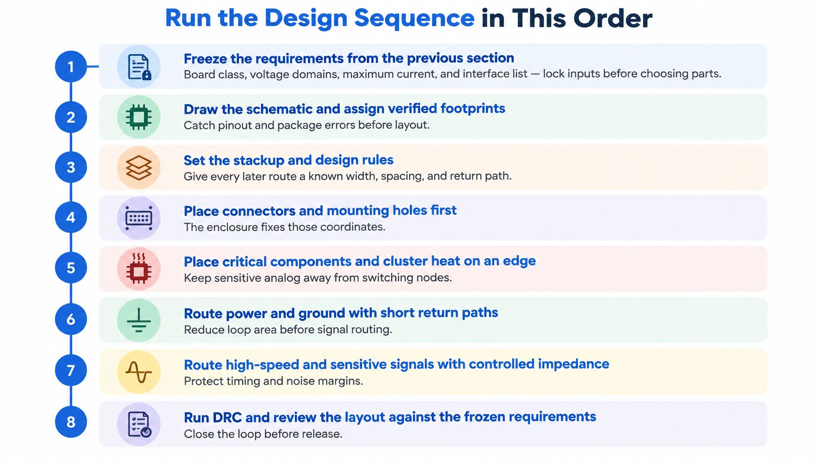
PCB layout works best as a controlled sequence with explicit handoffs. AdvancedPCB's performance and manufacturability guidance connects requirements, stack-up, placement, routing, and manufacturing review rather than treating routing completion as the finish line.
Use the process flow as a review aid, with critical routing prioritized according to the product's electrical risks.
<a id="complete-each-handoff-before-committing-the-next"></a>
Complete each handoff before committing the next
-
Freeze requirements before selecting implementation details, because changing the envelope, current demand, or interface list later can invalidate the layout. Include electrical limits, environmental conditions, assembly technology, and acceptance requirements. Resolve contradictory inputs rather than hiding them in fabrication notes.
-
Capture and electrically check the schematic before placement, because a correct layout can faithfully reproduce an incorrect circuit. Give each signal a consistent net identity, make power domains explicit, and review hidden supply pins. Resolve schematic-to-layout mismatches before routing.
-
Select components and verify footprints while assembly choices are still flexible. Compare package drawings with pad numbering, orientation, exposed-pad treatment, and courtyard dimensions. Fine-pitch QFN and BGA packages also require an escape, stencil, and inspection strategy, not merely a matching footprint name.
-
Build the stack-up with the fabricator before setting impedance widths, because material availability and process capability constrain the geometry. Put the agreed copper and dielectric information into the CAD layer model. Save the approved revision alongside the constraint sheet.
-
Place connectors and mounting holes before arranging movable circuitry, because the enclosure fixes their coordinates. Then organize heat-generating devices, switching circuitry, and sensitive analog or RF blocks. Leave space for their return paths and test access, not just their component bodies.
-
Route the electrically critical networks before consuming routing channels with ordinary signals. Protect controlled-impedance paths and differential pairs, and size power conductors using IPC-2152 methodology rather than a universal width rule. Where a power stage is the dominant risk, establish its compact current loops before completing nearby signals.
-
Finish ordinary signals without relaxing the approved geometry to make the last connection fit. Check plane neckdowns, copper islands, thermal reliefs, and via-field congestion while routing. A completed airwire count doesn't show whether the remaining plane copper can carry the intended return or load current.
-
Run the release reviews after the final copper update, because earlier results become stale when pours or routes change. Include DRC, plane connectivity, return-current review, mechanical clearance, impedance review, and fabricator DFM. Close every waiver with an owner and a reason.
<a id="recognize-order-dependent-failures"></a>
Recognize order-dependent failures
Consider a hypothetical IoT board whose regulator occupies the cleanest routing corridor before the antenna network is placed. The engineer can still finish every connection, but the resulting RF route may pass beside switching copper or lose its intended reference. Continuity testing won't reveal that placement mistake.
Route completion proves that the nets connect. It doesn't prove that you preserved the electrical conditions those nets need.
For a visual walkthrough of PCB design operations, use the accompanying demonstration.
<iframe width="100%" style="aspect-ratio: 16 / 9;" src="https://www.youtube.com/embed/PMEpQZ90f34" frameborder="0" allow="autoplay; encrypted-media" allowfullscreen></iframe><a id="place-hot-noisy-and-quiet-circuits-apart"></a>
Place Hot Noisy and Quiet Circuits Apart
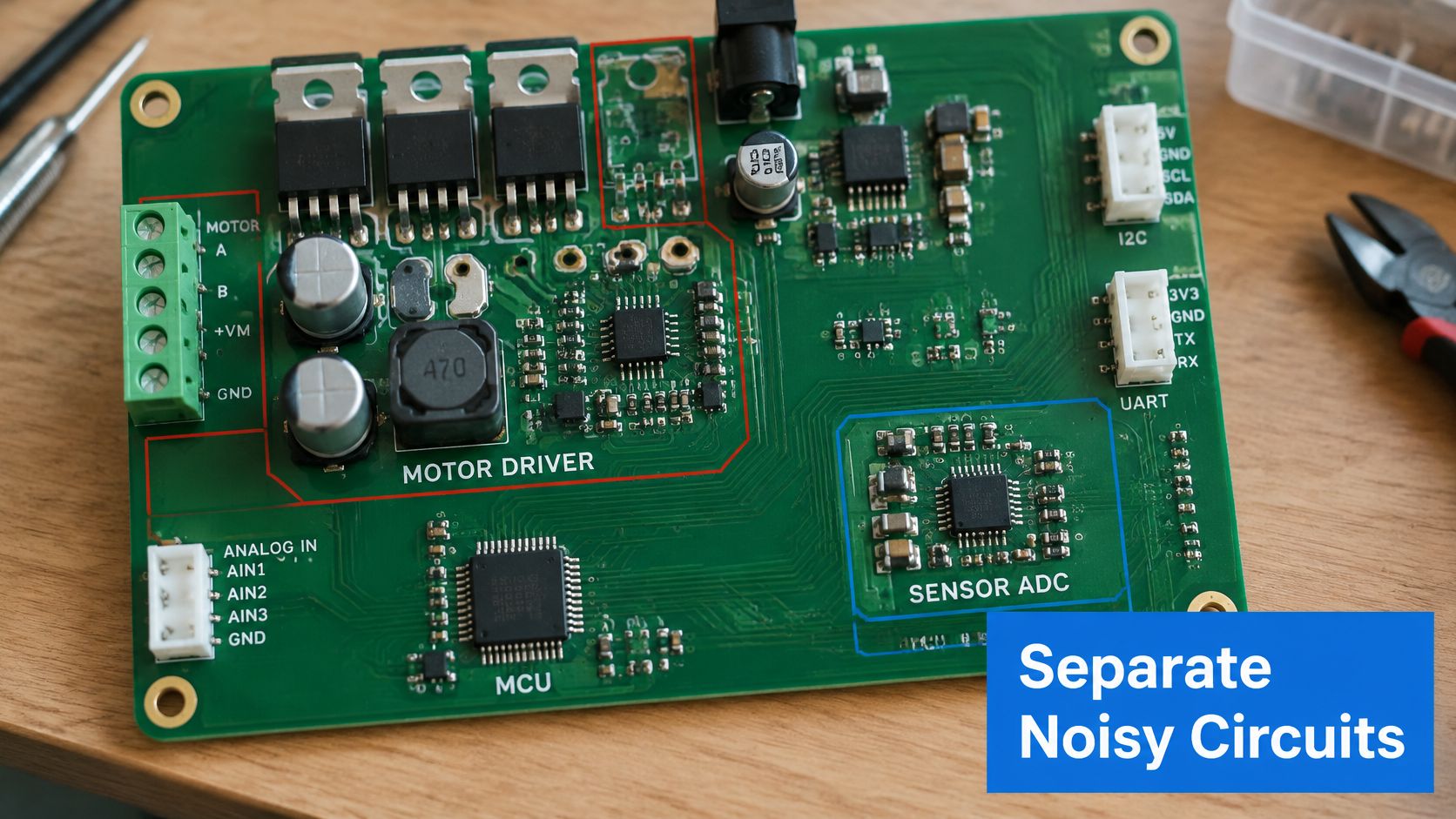
Consider a motor driver sharing a board with a precision sensor ADC. The useful division isn't “digital on one side, analog on the other.” It's high-current switching loops separated from sensitive measurement paths, with deliberate return-current routing.
The board photograph illustrates the component-density problem; the electrical floorplan must also account for copper and current paths beneath those components.
<a id="follow-the-current-around-the-floorplan"></a>
Follow the current around the floorplan
Start at the motor connector and trace the load-current path through the driver, supply bypass network, and return. Place the switching devices and local capacitors to keep the rapidly changing current loop compact. Keep the switch-node copper no larger than the electrical and thermal design requires.
Place the ADC near its input conditioning and reference components. Route sensor returns so motor current doesn't flow through the same narrow copper used to establish the measurement reference. Where current sensing requires Kelvin connections, take the sense traces from the intended resistor terminals rather than convenient points on the power pour.
Don't split the ground plane merely to make the analog and power regions look separate. Use component placement and routing to control current paths while maintaining the reference continuity required by fast signals.
For heat, identify the complete route from junction to ambient or chassis. Position the driver over an engineered copper and via structure, or near a suitable heat-spreading interface. An enclosure edge is helpful only if the mechanical design provides a heat-transfer path there.
<a id="reserve-space-for-assembly-and-observation"></a>
Reserve space for assembly and observation
BGA escape routing should be tested before surrounding circuitry consumes the available channels. Model critical escape transitions, and keep switching nodes away from crystals, antenna feeds, and analog-reference traces. Moving a sensitive trace away from the aggressor is usually more useful than making it wider without analysis.
Add inspection and test features during placement:
- Power access: Provide probe locations for each rail and a usable ground connection beside them.
- Hidden joints: Reserve the access and fixture geometry needed for the chosen X-ray or functional-test strategy.
- Assembly references: Include the fiducials and panel-related clearances agreed with the assembler.
- Mechanical clearance: Check actual component bodies, connector mating space, fasteners, and enclosure bosses in the mechanical model.
If you can't identify the outgoing current and its return on the floorplan, the placement review isn't complete.
Before approving placement, check connector coordinates, heat-transfer interfaces, switching-loop area, sensitive-signal corridors, package escapes, and test access together. Otherwise, the last routing task becomes a negotiation over space that should never have been consumed.
<a id="prove-reliability-beyond-a-clean-drc"></a>
Prove Reliability Beyond a Clean DRC
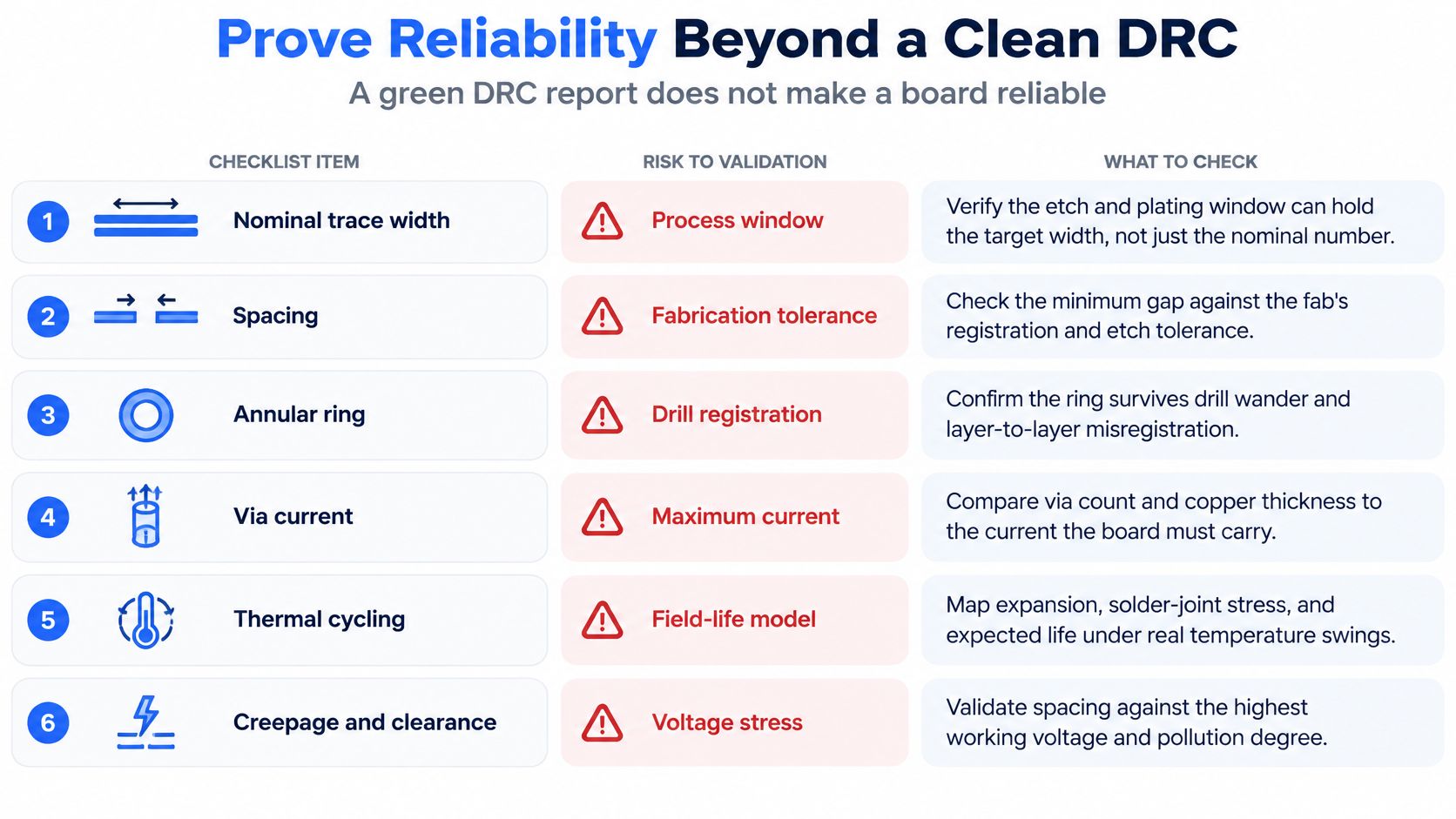
A green DRC report doesn't make a board reliable. It shows that the layout satisfies the rules configured in the tool. It doesn't demonstrate that the fabrication process can hold those rules across variation, or that the construction will survive the product's service conditions.
Treat the reliability checklist as a set of questions requiring evidence, not another collection of boxes to tick.
<a id="pair-the-construction-with-its-proof"></a>
Pair the construction with its proof
Standards-oriented coverage of advanced PCB construction identifies microvia structures, dynamic flex, and demanding signal-integrity requirements as areas needing more than nominal geometry checks in this technical paper on PCB reliability challenges. Convert those risks into requirements that appear in the drawing, qualification plan, or test specification.
| Construction or feature | Layout rule to freeze | Validation that proves it | |---|---|---| | HDI microvias | Approved via structure, layer connections, and fabrication limits | Representative via coupon and agreed reliability qualification | | Dynamic flex | Bend radius, moving region, bend direction, and copper arrangement | Bend testing at the intended radius and motion profile | | High-current region | Conductor geometry, via structure, copper thickness, and thermal boundary | Loaded temperature-rise measurement under defined conditions | | Controlled-impedance channel | Approved stack-up, geometry, and transition limits | Impedance coupon and appropriate channel measurements | | Hidden QFN or BGA joints | Land pattern, paste strategy, courtyard, and test provisions | X-ray where appropriate, supported by electrical or functional testing |
A stacked microvia structure and a staggered structure shouldn't receive interchangeable approval merely because both fit the escape. Ask what construction the qualification vehicle represents. Similarly, a static flex that bends once during installation doesn't establish the life of a continuously moving flex.
<a id="write-acceptance-criteria-before-building"></a>
Write acceptance criteria before building
NASA's Goddard PCB quality standard specifies IPC-2221 Class 3 design with applicable sectional standards, manufacturing and testing under IPC-6011 and companion requirements, and, for higher-risk mission classes, source inspection and review of the previous two years of production-lot quality history.
Commercial teams don't need to adopt a space-mission specification wholesale. They should adopt the discipline: translate service conditions into constraints, select a suitable construction, verify the process window, and document the manufacturing review.
Use the PCB design standards guide to organize the applicable design, performance, and acceptance documents. Keep their roles distinct, and specify the revisions the supplier must use.
For every validation, name the sample, operating condition, pass criterion, and responsible reviewer. “Check thermals” isn't sufficient; “measure the driver region at maximum specified continuous load in the production enclosure” is a test someone can execute.
<a id="fix-boards-that-pass-and-still-fail"></a>
Fix Boards That Pass and Still Fail
A board that passes netlist comparison but fails EMC needs an investigation of current paths, not an immediate collection of extra capacitors. Identify the noisy source, the sensitive circuit or cable, and the coupling path. Change the geometry that created the problem before adding parts without a diagnosis.
Symptoms that survive a connectivity test
| Symptom | Likely layout cause | Fix | Respin or note | |---|---|---|---| | Fails EMC, passes netlist | Interrupted return or victim trace beside switching copper | Restore the reference path and relocate the victim | Copper respin | | Closed eye on a serial link | Excessive stub, unnecessary transitions, or incorrect dielectric model | Reduce the offending stub and rerun the channel model | Respin or approved backdrill change | | Trace hotter than expected | Width based on the wrong copper thickness or layer conditions | Recalculate and resize the conductor | Width respin | | Hidden-joint yield loss | Unsuitable paste design, assembly clearance, or inspection plan | Review paste deposition and joint inspection | Assembly change, with respin if geometry prevents correction | | Flex cracks in use | Unsuitable bend geometry, copper arrangement, or unspecified motion | Redesign the bend region and qualify the intended motion | Flex respin | | Coupon misses impedance | Fabricated width or dielectric differs from the model | Reconcile the measured construction with the approved stack | Fabrication correction or revised geometry |
<a id="separate-copper-problems-from-process-problems"></a>
Separate copper problems from process problems
Treat the table as a set of hypotheses, not automatic diagnoses. A closed eye can also involve connectors, terminations, or device settings. Compare measurements with the model before authorizing a board change.
An impedance miss doesn't disappear because someone edits a fabrication note. Measure the actual trace cross-section and dielectric construction, determine which assumption was wrong, and correct either the fabrication process or the design.
Revision discipline: Change the artifact responsible for the failure, not whichever file is easiest to edit.
For assembly defects, review paste inspection and joint evidence before respinning copper. A stencil adjustment may solve deposition problems, while inadequate courtyard clearance requires a physical redesign.
Log the failed assumption beside the constraint sheet, including the measurement that disproved it. That record prevents the next revision from inheriting the same unverified default.
<a id="release-the-package-and-ask-for-dfm"></a>
Release the Package and Ask for DFM
Release is a consistency check, not a file-export event. Compare Gerber or ODB++, drill data, the approved stack-up, fabrication drawing, netlist, BOM, and pick-and-place files. If they describe different revisions, don't place the order.
<a id="close-the-release-checklist"></a>
Close the release checklist
- Fabrication agreement: Confirm materials, acceptance class, impedance requirements, drill definitions, and coupon instructions.
- Assembly agreement: Confirm substitutions, polarity, component rotations, paste requirements, and hidden-joint inspection.
- Validation agreement: Assign prototype measurements, fixtures, pass criteria, and responsibility for reviewing results.
Include native CAD files when the reviewer needs design intent that manufacturing outputs don't preserve. Our contact process accepts Gerber, ODB++, Altium, Eagle, or KiCad attachments up to 20 MB.
Our workflow starts with Gerber, BOM, and pick-and-place submission through a secure portal. Engineers review design and component availability before quotation; manufacturing, assembly, testing, and worldwide shipment follow approval.
Use the PCB fabrication service overview to prepare the handoff. Begin with a prototype build and its validation plan rather than treating volume production as the first experiment. Submit only when the constraint sheet, coupon plan, netlist, and manufacturing outputs agree.
Lianyuhong Technology Co.,Ltd offers schematic capture, PCB layout, SI/PI simulation, DFM review, fabrication, and assembly to connect design decisions with the finished build. Visit Lianyuhong Technology Co.,Ltd to submit your design package for engineering review, including the construction requirements and validation checks your prototype must prove.