
You've finished your layout, you've checked your clearances, and now you're staring at three quotes that don't look comparable at all. One is for bare boards, one adds assembly, and one assumes someone else is buying parts. That's the moment most buyers realize a PCB fabrication service isn't a fixed product. It's a scope of work, and the files and choices you send shape the price as much as board size does.
Table of Contents
- What a PCB Fabrication Service Actually Covers
- Service Models Compared From Bare Board to Full Turnkey
- Matching Your Project Stage to the Right Service
- Board Types and the Capabilities Behind Them
- Impedance Tolerance and How to Prove It
- How a Board Moves Through Production, Step by Step
- Confirm Your Provider Before You Order
<a id="what-a-pcb-fabrication-service-actually-covers"></a>
What a PCB Fabrication Service Actually Covers
A prototype arrives with clean traces and plated holes, but the microcontroller is still in its packaging and the board has not been tested as a working unit. That can be the expected result: the order covered bare-board fabrication, not assembly.
<a id="what-fabrication-means-in-practice"></a>
What fabrication means in practice
PCB fabrication turns the board design into a bare board. The manufacturer builds the layer stack, forms and plates holes, patterns the copper, and applies solder mask and a surface finish. Electrical testing checks that the intended connections are present and unwanted shorts are absent.
Fabrication works like baking the bread; assembly adds the fillings, and a turnkey order delivers the finished sandwich. The terms describe different scopes, so a quote for bare boards cannot be compared directly with one that also includes parts and assembly.
The files and choices in your request shape the quote. Stack-up approval affects the materials and layer construction; the accepted file format affects how the design is prepared for production. If assembly is included, the sourcing model and requested test scope also affect cost and lead time. Board size matters, but it is only one part of the specification.
Before requesting a quote, list the work you need: fabrication, design review, component sourcing, assembly, testing, and shipping. Ask the provider to identify which items are included, then confirm that the quoted stack-up and production files match your intended build.
<a id="service-models-compared-from-bare-board-to-full-turnkey"></a>
Service Models Compared From Bare Board to Full Turnkey
Four models cover most orders, and each hides the same decision, who supplies the boards, who sources the components, and who carries inventory risk if a part goes obsolete or a build gets delayed.
| Model | Board supply | Component sourcing | Inventory risk | Best fit | |---|---|---|---|---| | Bare board fabrication only | Provider fabricates the PCB | Customer buys all components | Customer holds all component risk | Teams with purchasing staff and in-house assembly | | Consigned full kit | Customer supplies boards and components | Customer kits parts, provider assembles | Customer holds inventory | Teams with stocked parts and a steady assembly partner | | Partial turnkey | Provider fabricates boards and sources hard-to-find parts | Customer supplies the remaining parts | Shared between both sides | Projects blocked by one or two scarce components | | Full turnkey | Provider fabricates boards | Provider buys and manages all components | Provider holds component inventory | Startups and OEMs wanting one accountable partner |
<a id="bare-board-only-and-consigned-kit"></a>
Bare board only and consigned kit
Bare board only suits you if you've got purchasing staff and your own assembly line. You control every part number and every supplier, but you also own every shortage. If a reel arrives late, your line waits, and there's no one else to call.
Consigned full kit keeps you in control of parts while someone else does the placement work. You kit the components, ship them with the boards, and the provider assembles. It works well when you've already got stocked parts from a previous build, though the kitting, counting and shortage checking all land on your team.
<a id="partial-turnkey-and-full-turnkey"></a>
Partial turnkey and full turnkey
Partial turnkey splits the sourcing. We fabricate the boards and source the hard-to-find components, you supply the rest, and inventory risk is shared. That's the right shape for a project blocked by one scarce FPGA or an allocated sensor, because you don't hand over sourcing for parts you can already buy easily.
Full turnkey gives you one point of accountability and one quality system. We handle bare board fabrication, component sourcing and full assembly under one roof, and we hold the component inventory. The trade-off is larger upfront component purchasing on our side, which you'll see reflected in payment terms.
We offer all three engagement models, turnkey, consigned full kit and partial turnkey, so the same board can move between them as your project matures. A prototype might start consigned with parts from your lab stock, then shift to turnkey once the design settles. Ask yourself which constraint dominates right now, scarce parts, thin purchasing capacity, or the need for one accountable partner. That answer picks the model.
<a id="matching-your-project-stage-to-the-right-service"></a>
Matching Your Project Stage to the Right Service
The right service follows your project stage more than your board dimensions. A small board at production volume needs a different contract than a large board at proof of concept, because what you're buying changes from speed to repeatability to supply continuity.
| Project stage | Typical quantity | What matters most | Service tier to choose | |---|---|---|---| | Proof of concept | 1 to 10 boards | Speed and fast design iteration | Quick-turn fabrication with low or no MOQ | | Engineering validation | 10 to 100 boards | Prototype stack-up matching production | Turnkey prototype assembly with DFM review | | Pilot or low volume | 100 to 1,000 boards | Repeatable yield and documented parts | Low-volume turnkey assembly with test coverage | | Production | 1,000 boards and above | Unit cost, traceability and supply continuity | Full turnkey or consigned model with a contracted quality system |
Treat those quantities as planning ranges, not rules. A complex HDI board might still be a proof of concept at twenty pieces, while a simple two-layer controller can be in production at five hundred.
<a id="early-stages-where-speed-misleads"></a>
Early stages where speed misleads
At proof of concept, speed and iteration dominate. Quick-turn fabrication with a low or no minimum order quantity fits, but confirm the MOQ before you order, because a cheap per-board price means little if you're forced to buy hundreds. Our turnkey assembly has no MOQ and covers prototype to production, and we offer quick-turn assembly for early builds.
At engineering validation, a faster prototype can hurt you. If a prototype service substitutes a different laminate or prepreg to hit a ship date, your validation results describe a board you won't sell. The prototype stack-up must match production, so get material substitutions approved in writing or refuse them.
<a id="later-stages-where-records-matter"></a>
Later stages where records matter
In a pilot run, ask for test coverage detail and component traceability, because repeatable yield and documented parts are what you are proving. At production, unit cost matters, but a contracted quality system and a plan for component continuity matter more over a product's life.
Say a team validates a sensor board, then orders a pilot of several hundred units. If the stack-up approved at validation doesn't carry into the pilot, the pilot yield data won't predict production yield. Match the tier to the stage you're in now, and plan the move to the next tier before you place the first order.
<a id="board-types-and-the-capabilities-behind-them"></a>
Board Types and the Capabilities Behind Them
A capability list on a website tells you what a provider offers. The capability check in the last column tells you what to verify before you trust it.
| Board type | Typical layers | Common applications | Capability to verify | |---|---|---|---| | FR-4 rigid | 1 to 24 layers | Consumer, IoT, industrial controls | Impedance control and layer registration | | HDI | Multilayer with laser microvias | Smartphones, wearables, BGA-dense designs | Microvia type, registration and approved stack-up | | Flexible FPC | 1 to 8 layers | Cables, folding sensors, compact connections | Bend radius and coverlay accuracy | | Rigid-flex | 2 to 14 layers | Foldable instruments, camera modules | Rigid-to-flex transition design and bend zones | | Metal core | Usually 1 to 2 layers | LED lighting, motor drivers | Dielectric thermal performance and aluminum or copper base | | High-frequency | Multilayer on Rogers, PTFE or Taconic | RF, microwave, telecom equipment | Laminate stability and hybrid stack-up | | Ceramic | Usually 1 to 2 layers | Power modules, high-temperature circuits | Substrate thickness and metallization adhesion |
Our published ranges are FR-4 and high-layer-count rigid boards at 1 to 24 layers with impedance control, flexible circuits at 1 to 8 layers, and rigid-flex at 2 to 14 layers. FR-4 stays the default because it's the workhorse laminate. Most cost and lead-time comparisons start there, and you should move to a specialty material only when heat, flexibility or frequency forces the move. Our overview of PCB manufacturing techniques shows how those board families are built differently.
<a id="why-hdi-is-a-reliability-question"></a>
Why HDI is a reliability question
Buyers often shop HDI by minimum feature size, the smallest trace or via on a brochure. That's the wrong test. A board can hit a fine feature size once and still fail after thermal cycling in the field.
The ProtoExpress guide to IPC standards for PCB designers notes that IPC design guidance covers material selection, electrical properties, thermal management, physical construction, interconnections and documentation, while production validation commonly uses test coupons and microsection analysis. HDI should be specified around interconnect reliability, because laser microvias, blind and buried structures, sequential lamination and back-drilling stack process tolerances on top of each other.
Here's the mechanism. Poor registration between layers or thin plating in a microvia leaves little margin, so thermal expansion during reflow and use can crack a barrel or open a joint intermittently. An uncontrolled via stub acts differently, it creates resonances that degrade signal integrity before any assembly defect is visible, which is why back-drilling needs a controlled drill depth and a documented remaining-stub limit on your drawing.
Ask for a capability sheet listing layer count, minimum features, microvia type and high-frequency laminate options before you shortlist anyone. For HDI, add first-article cross-sections and microvia reliability evidence.
<a id="impedance-tolerance-and-how-to-prove-it"></a>
Impedance Tolerance and How to Prove It
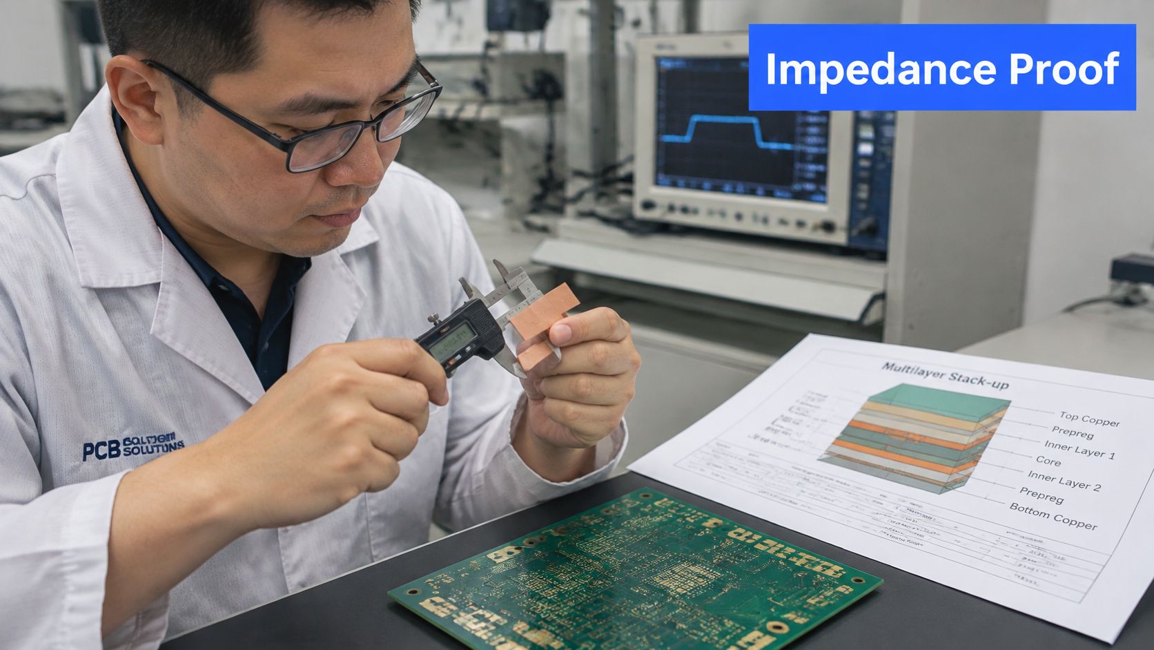
Controlled impedance is like a water pipe. Change the pipe's diameter or wall thickness and the flow changes, even if the route on the drawing stays identical. Your routed trace is the route. The factory's materials and pressing process decide the diameter.
That means controlled impedance is a stack-up and process specification, not just a routing rule you set in your CAD tool. Finished impedance depends on dielectric thickness, trace width, copper thickness, solder-mask effects, resin content and the laminate's effective dielectric constant. If a fabricator swaps a core and prepreg combination for one that's close on paper, your nominal CAD stack-up can miss its target.
<a id="what-tolerance-should-you-specify"></a>
What tolerance should you specify
The AES Techno guidance on PCB stack-up, impedance and EMC treats ±10% as a normal controlled-impedance fabrication tolerance and ±5% as a tighter, more costly requirement. Don't pay for ±5% by default. It's justified for RF, high-speed serial links and dense HDI only when your supplier can document stack-up control and measurement capability. Our notes on impedance control PCB design cover how those requirements get translated into a buildable stack-up.
<a id="three-documents-that-prove-it"></a>
Three documents that prove it
- Manufacturer-approved stack-up: Get it before routing, with the approved laminate family, finished copper thickness and dielectric heights after pressing. Route to real materials, not library defaults.
- Target list with a substitution ban: State the target impedance for every critical single-ended and differential net, plus trace-geometry assumptions, and prohibit unapproved material substitutions in writing.
- Coupon and cross-section results: Require impedance coupons on production panels, tested with TDR or an equivalent method. Cross-section analysis then confirms actual conductor width and dielectric geometry.
Those three documents prevent respins caused by insertion loss, reflection, crosstalk and eye-diagram failures. Assembly inspection can't fix those problems after the board is fabricated, because the fault is baked into the copper and dielectric. A coupon report costs little. A respin costs you a schedule.
<a id="how-a-board-moves-through-production-step-by-step"></a>
How a Board Moves Through Production, Step by Step
The diagram below compresses the flow into five stages, from file submission through final test.
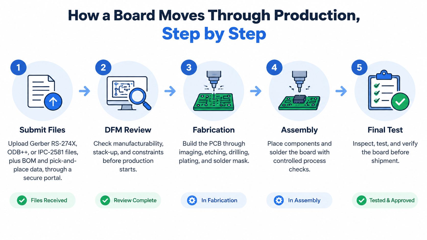
In the factory, those five stages break into nine practical steps.
- Submit your files: Send Gerber RS-274X, ODB++ or IPC-2581 files, plus your BOM and pick-and-place data, through a secure portal. We accept those three formats. The common slip here is exporting files without a defined layer stack, which forces the factory to guess your build.
- Run DFM review: Engineers check trace-to-hole clearance, annular ring, drill sizes, panel layout and component availability, then send feedback before anything is cut. Fixing a clearance in a file costs minutes. Fixing it in copper costs a remake.
- Approve the quote and stack-up: You receive a detailed quotation with transparent pricing and lead-time options, and you approve materials and impedance requirements. Skipping stack-up approval at this step is the second common slip, and it's the one that causes impedance surprises later.
- Image, etch and laminate inner layers: Inner copper patterns are printed and etched, then pressed together with prepreg into a multilayer core.
- Drill, plate and image outer layers: Holes are drilled and plated to connect layers, then outer circuits are imaged and etched.
- Apply solder mask, silkscreen and surface finish: Mask protects the copper, silkscreen adds reference marks, and a finish such as HASL or ENIG keeps pads solderable.
<a id="from-bare-board-to-shipped-assembly"></a>
From bare board to shipped assembly
- Test the bare board: A flying probe tester suits prototypes, while a fixed fixture suits volume. AOI inspection checks for etching and registration defects a continuity test can't see.
- Assemble the board: We print solder paste through a stencil, place components, and reflow under air or nitrogen. Our turnkey service includes nitrogen reflow, wave soldering and selective soldering, so through-hole parts get soldered after the surface-mount pass.
The video below shows how placement, reflow and inspection equipment move a panel through an assembly line.
<iframe width="100%" style="aspect-ratio: 16 / 9;" src="https://www.youtube.com/embed/Zm_-in6FvM4" frameborder="0" allow="autoplay; encrypted-media" allowfullscreen></iframe>- Inspect, test, pack and ship: X-ray checks hidden joints where needed, functional test confirms the board works as a circuit, and finished assemblies are packed and shipped worldwide.
Notice the order of our four-step ordering process behind those nine steps: upload files, get DFM feedback, receive the quotation, then we manufacture, assemble, test and ship. Steps one to three are when you still have control. After lamination, you're paying for changes instead of making them.
<a id="confirm-your-provider-before-you-order"></a>
Confirm Your Provider Before You Order
Your quote price reflects your file package more than your board area. An unapproved stack-up, a missing test scope or a late parts substitution can add respins and delays that outweigh a lower headline number, so confirm these five items before you compare prices. Our summary of PCB design standards is a useful reference while you prepare that package.
<a id="the-pre-order-checklist"></a>
The pre-order checklist
- File formats and DFM timing: Confirm accepted formats and whether DFM review happens before the quote, because clearance errors are cheapest to fix before fabrication starts.
- Impedance documents: If your board is controlled-impedance, get the approved stack-up and coupon reporting agreed before ordering, not after panels are pressed.
- Test scope: Ask what's included. Our assembly is full-turnkey SMT, THT and mixed assembly with BGA and fine-pitch support, handling 01005 to BGA and QFN components, with AOI, X-ray and FCT testing, because hidden BGA joints can't be judged by eye.
- Traceability and lead-time options: Ask how components are recorded and what happens when a part goes short, since substitutions found late cause the most delay.
- Quote scope: Check whether the price includes component procurement, stencil and test. Our PCB assembly starts from $0.008 per joint, but a per-joint figure only helps you compare when you know what else is bundled around it.
The single action that settles most of this: Send your Gerber, BOM and pick-and-place files for DFM review and a written quote, then compare quotes on scope rather than on the headline number.
Two quotes at different prices usually aren't two prices for one job. They're two different jobs. Once you've aligned file formats, stack-up approval, test scope and sourcing responsibility, the cheaper quote is finally a meaningful signal, and the more expensive one has to explain what extra risk it's removing for you.
Choosing a PCB fabrication service gets easier once your files, stack-up and sourcing model are settled, and that's exactly where we can help. Send your Gerber, BOM and pick-and-place files to Lianyuhong Technology Co.,Ltd for DFM review and a written quote covering fabrication, component sourcing, assembly and test, so you can compare scope with confidence and move from prototype to production without changing partners.