
You've got a board on the bench that powers up, beeps for continuity, and passes a quick functional check. Then someone plugs in a cable, the enclosure warms up, or the unit rides in a vehicle for a week, and it drops out. That pattern is classic for a solder cold joint, and it's why a shiny blob can still be a bad bond.
Table of Contents
- Signs That a Joint Never Really Bonded
- What a Cold Joint Actually Is
- Why a Weak Cold Joint Matters in Service
- Why the Joint Never Reached Flow Temperature
- Cold Joints Versus Joints That Only Look Wrong
- How to Rework a Cold Joint so It Holds
- Choose Rework or a Controlled Rebuild
<a id="signs-that-a-joint-never-really-bonded"></a>
Signs That a Joint Never Really Bonded
Start with a plain definition. A solder cold joint is solder that's present, but it never fully wet the pad and the lead, so the bond underneath is incomplete. The metal may touch today and still separate when the board flexes, vibrates, or changes temperature.
Inspect in a fixed order so you don't rely on one clue. First look at shape under magnification. A sound fillet is usually concave and feathers smoothly onto the copper, while a cold joint tends to sit up rounded, convex, or balled, as if the solder wanted to pull back rather than spread.
Next check surface and coverage together. Grainy, porous, or uneven gray texture suggests the solder didn't fully flow and coalesce, but don't convict a joint on dullness alone. Lead free fillets can look matte and still be perfectly wet, so coverage matters more. If solder stops short of the pad edge, climbs only partway up the lead, or leaves a sharp boundary, the bonded area is smaller than the blob suggests.
<a id="use-the-table-on-the-bench"></a>
Use the Table on the Bench
| Sign | Cold joint | Sound joint | What it implies | |---|---|---|---| | Fillet shape | Rounded, convex, or balled up | Concave fillet that feathers onto the pad | Solder melted but did not spread | | Surface | Grainy, porous, or uneven gray | Smooth and even; lead free may be matte | Incomplete flow and coalescence | | Wetting coverage | Stops short of pad edge or lead | Wets pad and lead around the perimeter | Bonded interface is smaller than it looks | | Mechanical check | Shifts or lifts with a light probe | Stays seated; lead is anchored | Little true metallurgical grip | | Electrical check | Beeps now, opens under flex, heat, or vibration | Stable through handling and thermal change | Intermittent contact, not a proven joint |
Now add two quick functional checks, gently. A light probe or careful tug with tweezers shouldn't move a properly anchored lead, but don't force it and lift a pad while you're testing. Compare resistance with a sister joint if you can, and watch whether the reading changes when you flex the connector or warm the board. A beep alone only proves a momentary path.
Bench rule: Mark any joint that fails two or more rows before you touch the iron. One dull surface can mislead you. A rounded fillet plus short coverage plus movement tells a much clearer story.
<a id="what-a-cold-joint-actually-is"></a>
What a Cold Joint Actually Is
Think about water on a pan. On a clean, warm pan, water sheets out and covers the surface. On a cold, greasy pan, it beads up in separate drops. Solder behaves the same way when it meets metal that isn't hot enough or isn't clean enough.
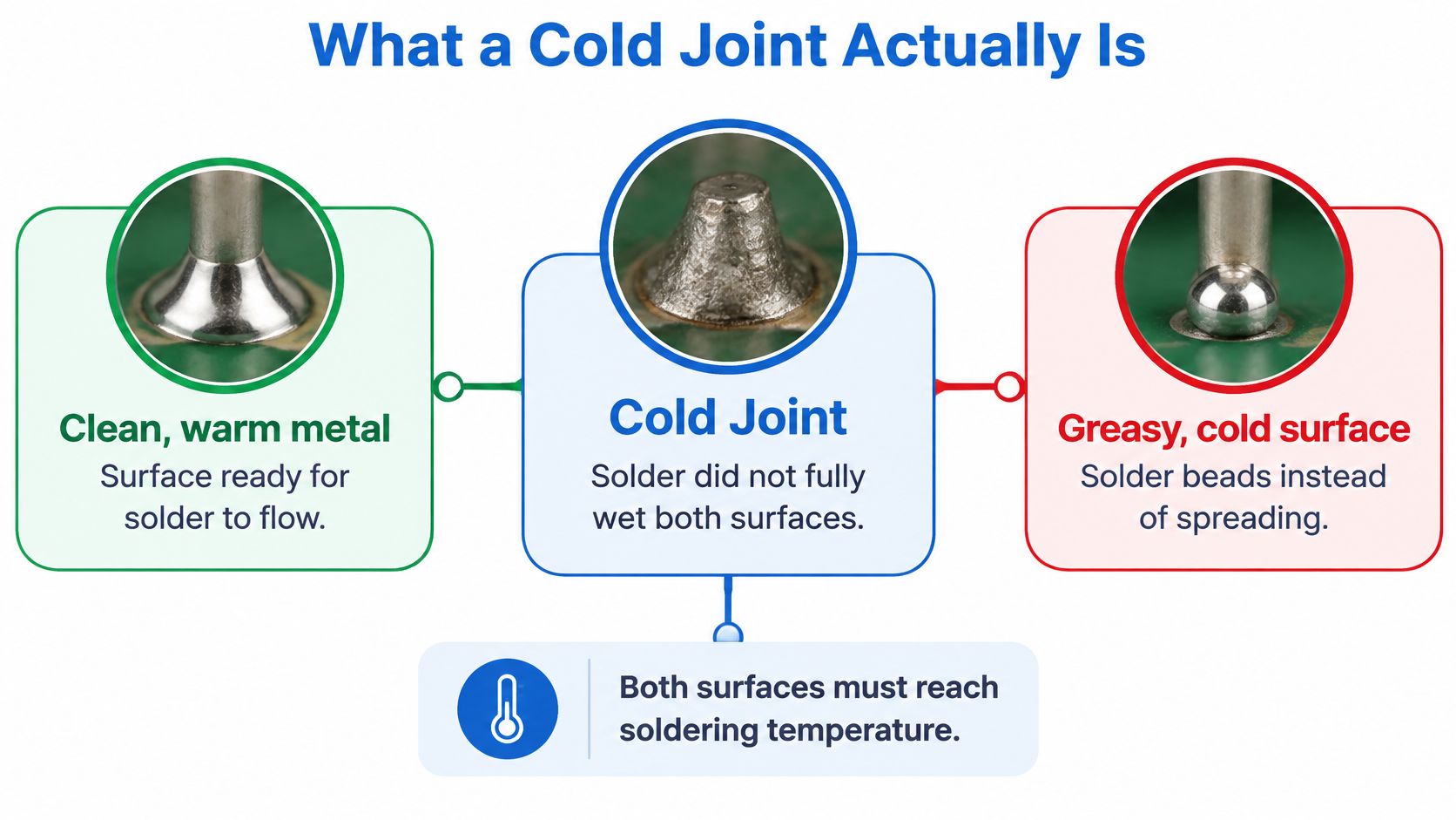
For a real joint, both surfaces have to reach the alloy's flow temperature. That's the component lead or termination and the PCB pad or barrel. If you heat only the solder wire, it melts in the middle and lands as a blob. It hasn't bonded to the cooler surface underneath.
Flux can't finish its job in that situation either. Flux needs heat and time to clear oxides so clean solder can meet clean metal. When one side stays cool, oxides remain, spreading stops, and you get a partial interface that looks filled from above. The outside can look generous while the true bonded area is a fraction of what you see.
<a id="the-workmanship-definition"></a>
The Workmanship Definition
That picture matches the formal definition. The NASA Student Handbook for Hand Soldering defines a "cold solder connection" as one with poor wetting and a grayish, porous appearance, and it requires solder to wet all connection elements and form a fillet around the complete connection perimeter. In plain language, acceptable solder has to grip every surface it claims to join.
That's why this defect isn't cosmetic. Incomplete wetting shrinks the contact area, so electrical resistance rises and mechanical strength falls before you see a crack. A joint can conduct at room temperature, then open when a connector is pushed sideways or the assembly expands during warm up. The weakness is built in at the moment the solder freezes.
Don't confuse that with a lead free joint that looks less bright than an old tin lead joint. Color is a clue, not a verdict. A matte fillet that feathers onto the pad and wraps the lead can be sound. A bright, rounded ball that sits beside bare copper is not.
The same failure shows up in different processes for the same reason. In hand soldering, the iron often heats the wire instead of the joint. In reflow and wave soldering, a heavy ground pad, connector shell, or through hole barrel may never reach liquidus even though smaller parts nearby look fine.
So inspect for the right thing. Don't ask only whether solder is visible. Ask whether it wet both surfaces and formed a continuous fillet around the perimeter.
<a id="why-a-weak-cold-joint-matters-in-service"></a>
Why a Weak Cold Joint Matters in Service
A cold joint matters because service conditions test exactly what it lacks, area and strength. The peer reviewed review in Chinese Journal of Mechanical Engineering reports that approximately 70% of electronic device failures originate during packaging, with solder joint failure identified as a principal contributor. A cold joint is an early, preventable form of that packaging failure.
The technician photo below shows the stage where that reliability is won or lost, at the joint interface itself.
Say a through hole connector is plugged in every day. Each insertion flexes the pins slightly. A sound fillet distributes that movement, while a grainy, partly bonded fillet concentrates stress on the small area that gripped. It works during final test and then starts dropping out in the customer's hands.
<a id="heat-and-vibration-finish-the-job"></a>
Heat and Vibration Finish the Job
Power parts create a different route to failure. An LED or regulator pad on thick copper heats and cools with load. The PCB, component, and solder expand at different rates, creating cyclic strain. Creep dominates during temperature dwells, and fatigue is especially important during temperature ramps, so a weak interface deteriorates even without someone touching it.
That sensitivity is sharp. In the SnAgCu thermal cycling study summarized in that review, increasing stress from 16 to 20 MPa reduced characteristic life by about 50%, and at 24 MPa the reduction approached 70%. Those figures aren't a universal cold joint failure rate. They show how quickly life falls once stress acts on an interface that already has less bonded area to share the load.
The risk climbs further when you can't see the joint at all. Fine pitch and bottom terminated parts need the inspection discipline described in our guide to BGA PCB assembly, because an automotive or industrial board can pass power up and then fail under combined heat cycling and vibration.
This short video walkthrough is useful for connecting the bench appearance to the service failure you are trying to prevent.
<iframe width="100%" style="aspect-ratio: 16 / 9;" src="https://www.youtube.com/embed/VLubdi6aC3g" frameborder="0" allow="autoplay; encrypted-media" allowfullscreen></iframe>Care most where cycles and consequences stack up. High cycle connectors, high temperature power boards, automotive and industrial hardware, and hidden BGA or QFN joints deserve prevention and inspection, not optimism.
<a id="why-the-joint-never-reached-flow-temperature"></a>
Why the Joint Never Reached Flow Temperature
Cold joints usually come from one of three failures. The heat didn't get into the joint, the surface wasn't clean when the heat arrived, or the machine profile never gave the coldest pad enough time above liquidus. Grouping causes that way keeps you from changing five settings at once.
<a id="hand-soldering-loses-heat-at-the-tip"></a>
Hand Soldering Loses Heat at the Tip
An oxidized tip transfers heat poorly even when the station display looks correct. A small conical tip can also be the wrong tool for a wide tab or ground pin, because its contact patch is too small to keep up. The part the reader touches is the joint, not the display, so a clean, tinned tip with real contact area matters.
Technique can defeat a good station. If you melt wire on the iron and carry a drop to a cold pad, the solder is liquid but the pad and lead aren't at flow temperature. Large ground planes, metal connector shells, and thick copper pours also sink heat away continuously. You have to heat the assembly, sometimes with board preheat, not just touch it longer with a failing tip.
Movement belongs here too, with a distinction you'll use later. If the lead shifts after proper flow while the solder is freezing, you've disturbed a joint that had started to form. That's related, but it isn't proof the surfaces never reached temperature.
<a id="the-surface-was-not-ready"></a>
The Surface Was Not Ready
Oxides, skin oils, old flux residue, and a degraded board finish consume flux before it can expose solderable metal. When flux is exhausted early, solder may melt and still refuse to spread. Cleaning the board, storing parts and bare boards properly, and questioning an old finish are thermal fixes in practice because they let the heat you apply produce wetting instead of a frozen bead.
<a id="reflow-profiles-miss-the-coldest-pad"></a>
Reflow Profiles Miss the Coldest Pad
Oven setpoints don't tell you what the heaviest pad experienced. The Indium reflow profile study reports that the minimum peak should be approximately 30°C above the solder's melting temperature, and operating closer to the melting point increases the likelihood of cold joints and insufficient wetting. Since SAC305 melts near 217°C, that principle implies a nominal peak around 247°C, within component, laminate, finish, and supplier limits.
Profile with thermocouples on the parts most likely to lag. Put them on large copper areas, heat sunk connectors, and shadowed components, not only on an easy corner of bare board. A short soak can leave flux underactivated, fast conveyor speed can shorten liquid time, and uneven copper can leave one region colder than the rest.
Wave and selective soldering fail the same way in barrels. If the pin and plated hole never reach flow, solder won't climb and wet the barrel properly, and raising pot temperature a little is a crude answer to a local heat transfer problem.
Use the pattern to narrow the cause. Defects clustered in one region point to thermal lag, shadowing, or copper imbalance. Random dull, poorly wet joints scattered across boards point more toward cleanliness, solderability, or operator technique.
<a id="cold-joints-versus-joints-that-only-look-wrong"></a>
Cold Joints Versus Joints That Only Look Wrong
Naming the defect correctly prevents the two most common wrong fixes, adding solder and turning up the heat. Use this comparison first, then read the pairs people confuse most often.
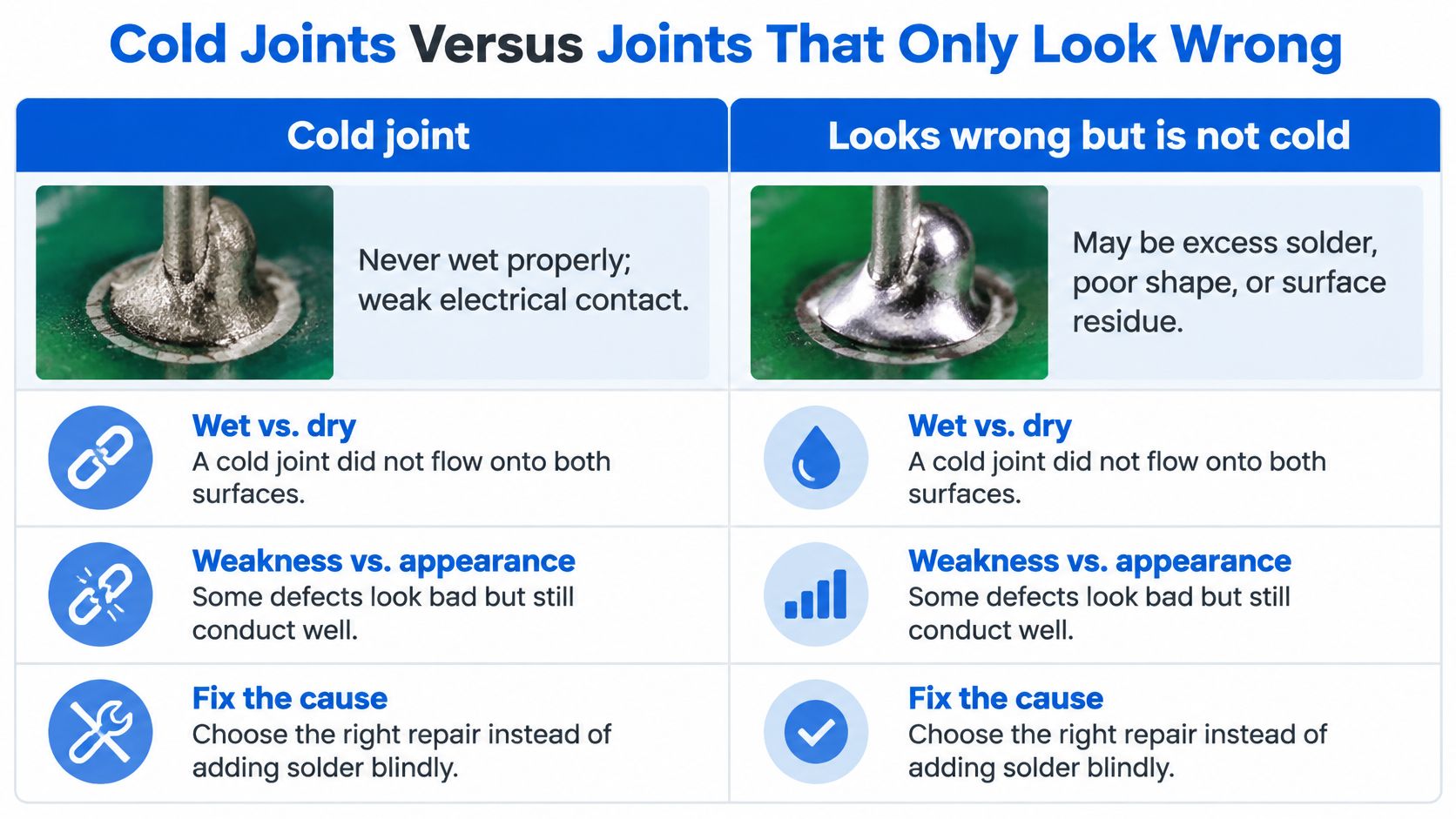
| Defect | Typical look | What failed | Matching fix | |---|---|---|---| | Cold joint | Grainy, rounded, incomplete wetting | Pad or lead never reached flow with a clean surface | Reheat both surfaces with flux; do not just pile on solder | | Disturbed joint | Dull, wrinkled, or cracked after it had flowed | Movement during solidification | Resolder and hold still until frozen | | Insufficient solder | Small but often shiny fillet | Too little paste or wire | Correct volume or stencil; heat is secondary | | Dewetting | Solder balls up after briefly spreading | Contamination or poor solderability | Clean or replace the finish; flux alone may not recover it | | Non wetting | Solder sits beside bare pad or lead | Oxide or unsolderable surface from the start | Abrade or replace, then flux and reflow | | Hidden void or open | Joint looks acceptable on top | Incomplete coalesce under BGA, QFN, or in a barrel | X ray or cross section, then profile or paste correction |
The IPC guidance document identifies insufficient heating and insufficient flux as principal causes, and it explains that poor wetting reduces joint strength, promotes voiding, and can produce no reliable joint at all. That's a cold joint, a failure to form the metallurgical bond in the first place.
A disturbed joint is different. It did wet, then the part moved while the solder was pasty, leaving a wrinkled or fractured texture over a real interface. Your fix is to remelt fully and hold everything still, not to investigate the board finish first.
<a id="starved-dewet-and-hidden-are-not-synonyms"></a>
Starved, Dewet, and Hidden Are Not Synonyms
An insufficient solder joint can be concave and bright because the small amount present wet very well. It needs volume, a stencil aperture correction, or more wire. More heat on a starved joint mainly cooks flux and risks pad damage.
Dewetting tells another story. Solder spreads briefly, then pulls back into islands, which points to contamination or a surface that can't sustain wetting. Non wetting never spreads at all. Those two look similar in a hurry, but they send you toward finish age, storage, and cleaning records rather than iron settings.
Hidden joints break the visual method completely. Voids or incomplete coalescence under a BGA or QFN, or inside a barrel, can't be judged by fillet color. Optical inspection is right for exposed fillets on a PCB assembly board, while buried interfaces need X ray or a destructive cross section when the evidence justifies it.
Name the defect before you choose the lever. Heat, flux, paste volume, and surface preparation fix different failures, and using the wrong one can make a recoverable board worse.
<a id="how-to-rework-a-cold-joint-so-it-holds"></a>
How to Rework a Cold Joint so It Holds
A cold joint failed to wet the first time, so rework has one job: make it wet now. A shiny blob can still be a bad bond, which is why every step below exists. Each one blocks a specific shortcut that recreates the original failure under a fresh cap of solder.
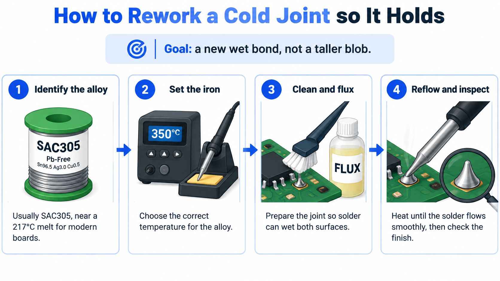
- Identify the alloy before setup: Modern lead free boards are commonly SAC305, and tin lead wets and freezes differently at the same tip temperature. Switching between alloys changes your iron settings, the dwell you should expect, and what a healthy fillet looks like, so confirm what is on the board before you touch the joint.
- Set up the iron: Use a temperature controlled station, a clean and freshly tinned tip, and a tip shape that can bridge pad and lead at once. A small chisel usually transfers heat better than a needle point on connector pins and ground pads.
- Add compatible flux: Put a small amount of fresh flux directly on the joint. The original flux was spent during the first pass, and relying on the core inside a long feed of new wire tends to add solder before it adds enough cleaning action.
- Heat pad and lead together: Set the tip so it contacts both surfaces, then wait until the old solder goes fully liquid and starts to move. Feeding wire too early melts the new metal while the interface underneath is still cold, which is the original defect in miniature.
- Remove bad solder when needed: If the old metal looks crusty, contaminated, or refuses to flow cleanly, wick it off with braid and inspect the pad. Building over rotten solder seals the failed interface under fresh metal, the same way paint over rust hides the problem instead of fixing it.
- Feed a little fresh solder to the joint: Touch the wire to the heated pad and lead junction rather than to the iron, and stop once solder flows onto both surfaces and feathers out into a concave perimeter fillet. Anything added after that is height, not grip.
- Freeze, clean, and prove it: Remove the wire first, then the iron, and hold the part still for several seconds while it solidifies. Clean the residue if your flux calls for it, inspect the full perimeter under magnification, then confirm the bond with a gentle mechanical nudge and a powered functional test.
<a id="edge-cases-that-change-the-method"></a>
Edge Cases That Change the Method
Heavy copper and connector shells often need board preheat so the iron isn't fighting the whole plane alone. That is standard practice on many jobs handled under through hole PCB assembly, especially ground pins tied to pours. Preheat also shortens tip dwell, which protects nearby plastic bodies and fine pitch leads.
Treat each pad as having a limited repair budget. Long dwell and repeated wicking can lift copper and damage mask, turning a cosmetic fix into a structural repair. If a cleaned, fluxed, properly heated pad still refuses to wet, stop and investigate the surface finish instead of applying more heat.
Hidden joints sit outside what hand rework can prove. Heating the edge of a BGA or QFN and hoping every ball reflowed leaves the actual interface unverified, so treat buried defects as a process problem rather than a touch up.
A successful rework collapses, spreads, and anchors. If the blob only gets bigger and shinier, you haven't fixed the interface yet.
<a id="choose-rework-or-a-controlled-rebuild"></a>
Choose Rework or a Controlled Rebuild
An isolated cold joint you can see and reach is a bench job. The same failure showing up at the same ground pin on board after board is a process problem. Choose by visibility, repetition, and consequence, and weigh the pattern across the whole board more heavily than one continuity beep.
<a id="three-questions-that-pick-the-branch"></a>
Three Questions That Pick the Branch
- Can you see and reach the whole joint? If the pad is intact, both surfaces are accessible, the component tolerates another heat cycle, and only a few joints failed, bench rework fits. Inspect the perimeter afterward and run a powered functional test before you call it done.
- Does the failure repeat in a pattern? The same connector row, ground region, or shadowed side failing across boards points at the process, and touching up each unit only spreads heat cycles around. Check tip condition, reflow profile records, flux age, board cleanliness, and paste volume before more boards go through the same setup.
- Is the joint hidden or the damage structural? Buried BGA, QFN, and barrel defects, lifted pads, and high-cycle or regulated hardware belong on a profiled rework station or in a replacement build. A hand pass cannot prove wetting you cannot see.
Fixing a repeating cold joint one pin at a time works like mopping the floor while the pipe still leaks. Watch for mixed defect types as well. Cold joints sitting next to disturbed or dewetted fillets usually share a root cause, and single-joint repairs leave that cause in place.
For a new lot, prevention means documentation you can audit. Ask for a recorded reflow profile measured on the heavy-copper areas, inspection criteria written around wetting, and X ray wherever joints are concealed. We perform SPI, AOI and X Ray inspection on every build, and offer flying probe and functional test, so paste deposition, visible fillets, hidden joints, and circuit behavior get checked as separate risks.
A prototype or small run that has already absorbed several touch ups can be cheaper to rebuild cleanly than to keep cycling through the iron. We offer quick turn PCB assembly and turnkey PCB assembly that includes bare board fabrication, component sourcing, and full assembly under one roof with one quality system and one point of accountability. Before you commit, ask any assembler, including us, for profiling records, inspection steps, and test coverage on your board type.
When the evidence points at the process, uploading your Gerber, BOM, and pick-and-place files at lyhcircuits.com starts an engineering DFM review of your design and component availability, followed by a detailed quotation with lead-time options.
If cold joints keep appearing in the same region, under hidden packages, or after repeated hand touch ups, treat it as a process problem and request a controlled rebuild. Lianyuhong Technology Co.,Ltd offers turnkey PCB assembly with SPI, AOI and X Ray inspection on every build, plus flying probe and functional test to catch wetting defects before boards ship. Start that review through Lianyuhong Technology Co.,Ltd.